In the previous article discussing purple fringing in photography, we mentioned that one of the sources of purple fringing is highlight overflow, known as the Blooming phenomenon.
Today, we will further elaborate on the Blooming phenomenon and the subsequent Smear phenomenon.
00 Preliminary Knowledge: Differences Between CCD and CMOS
Before explaining these two phenomena, let’s quickly review the differences between CCD and CMOS sensors.
a CCD
CCD stands for Charge Coupled Device, which is an abbreviation for charge-coupled device.
As the name suggests, this type of sensor uses a charge-coupled transfer mechanism for imaging.
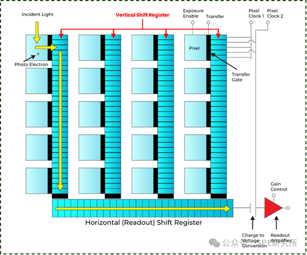
After light is converted into charge, it is transferred line by line to the edge amplifier for amplification and analog-to-digital conversion, turning the light signal into an electrical signal.
An imaging method is shown in the figure below:
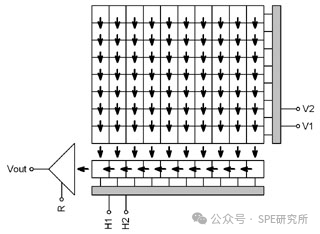
It can be simply understood that CCD reads the image information on the sensor line by line.
b CMOS
CMOS stands for Complementary Metal Oxide Semiconductor, which is an abbreviation for complementary metal-oxide-semiconductor.
This actually refers to a special process, and image sensors made using this process are also called CMOS sensors.
One characteristic of CMOS sensors in imaging is that each pixel integrates independent photodiodes, amplifiers, and ADC circuits. When reading image information, each pixel’s information is read independently, allowing for parallel processing to enhance reading speed, while the information of each pixel is less affected by surrounding pixels.
It can be simply understood that CMOS sensors read the information of each pixel independently at the same time and then combine this information in order.
Due to space constraints, we will write a detailed article later comparing the differences between CCD and CMOS.
For now, we just need to understand the differences in how these two sensors read image information.
01 Horizontal Blooming
First, let’s talk about the Blooming phenomenon.
In the previous article, we mentioned that the Blooming phenomenon is also known as highlight overflow.
This phenomenon refers to when there is an extremely bright point light source or area in the scene, the corresponding pixel in the sensor generates a number of photoelectrons that exceed the capacity limit of its charge storage area (potential well) due to excessive illumination, causing excess electrons to overflow into adjacent pixels.
I found an example image online, as shown below:
In the image below, a shows the imaging effect under normal conditions; b shows overflow in the vertical direction (this is what will be discussed as Smear), and c shows overflow in the horizontal direction.
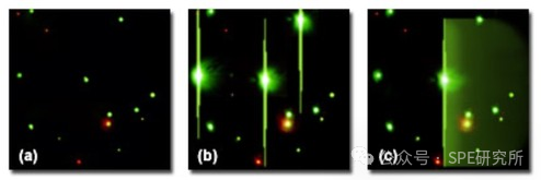
First, let’s discuss the overflow in the horizontal direction, which is Blooming.
In the previous article, when we mentioned this phenomenon, we simplified the illustration of the overflow for easier understanding, as shown in the figure below:
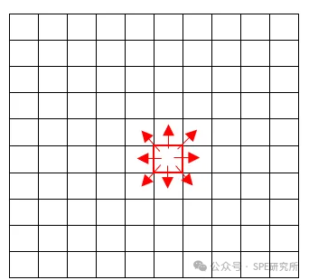
In reality, the Blooming phenomenon is more likely to occur in the horizontal direction, which is related to the imaging method mentioned above.
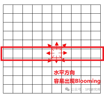
During imaging, the CCD first converts the light signal into electrons, which are then accommodated in the potential well.
Don’t ask, just know that I barely passed quantum mechanics with a score of 52, and only managed to pass during the retake.
Back then, the failure rate for this course was over 55%.
To assist understanding, it can be compared to the cup and water example I discussed in the previous article.
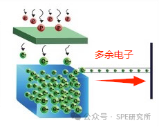
I found a schematic diagram online and translated it to show what happens at a single pixel during CCD imaging:
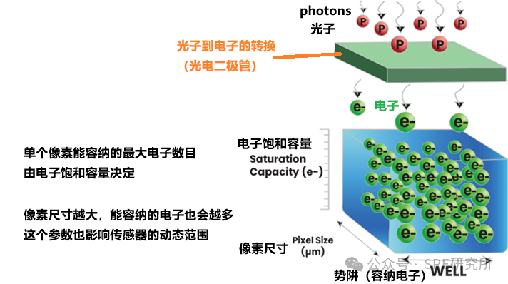
When a pixel is overexposed, it means that the electrons in the potential well are oversaturated and overflow, affecting the adjacent pixels in the horizontal direction:
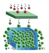
This leads to the phenomenon of horizontal Blooming.
02 Vertical Blooming — Smear
In certain special cases (or when Blooming is more severe), vertical Blooming phenomena may occur, as shown in the image above as b, manifesting as vertical bright lines or light bands across the frame.
This phenomenon is also known as the Smear phenomenon, commonly seen when photographing the sun or highly reflective objects.
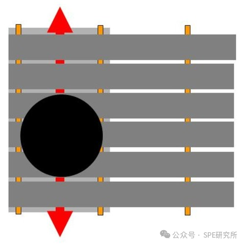
The cause of this phenomenon is that the electrons overflowing under strong light enter the vertical charge transfer register (the channel for CCD charge transfer) that should be shielded, or strong light is reflected/refracted into this area, causing an entire column of pixels to be “lit up.”
Another situation is that during the charge transfer period (on the order of microseconds), the photosensitive area continues to accumulate charge, contaminating the signal to be transmitted (especially noticeable during short exposures).
As shown in the figure below, the red part is the channel for CCD charge transfer:
03 Improvements in CCD
Both Blooming and Smear are harmful phenomena in photography.
These two phenomena can affect image quality, and in severe cases, impact practical applications. For example, in special scenarios like target recognition, such phenomena may lead to failure in target tracking.
Next, let’s discuss the improvements in CCD to avoid Blooming.
In fact, it is also possible to avoid overexposure by reducing exposure time, thus preventing the Blooming phenomenon.
Algorithms can also be used for post-processing to fix this.
When in doubt, just look for software.
a Avoiding Horizontal Blooming
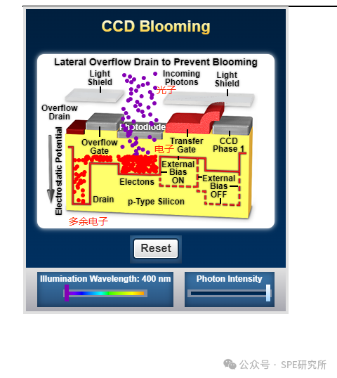
For the horizontal Blooming phenomenon, a common approach is to use Anti-Blooming Drains.
In simple terms, this actually provides a channel for electrons to transfer excess electrons, preventing overflow.
A more detailed diagram is shown below:
b Avoiding Vertical Blooming (Smear)
Avoiding the Smear phenomenon is relatively more complicated.
Common methods include reducing exposure time and narrowing the aperture to prevent overexposure.
It can also be achieved by reducing the CCD transfer time or using a mechanical shutter to block the light path during transfer to minimize the impact.
Of course, as mentioned above, the Smear phenomenon is a consequence of aggravated Blooming. If we can avoid the occurrence of Blooming, we can naturally avoid Smear to some extent.
04 Advantages of CMOS
The two phenomena mentioned above are common in CCDs, while in CMOS, due to structural optimization, they are basically unaffected by these two phenomena.
As shown in the figure below, each pixel in CMOS contains independent photodiodes, amplifiers, and discharge channels.
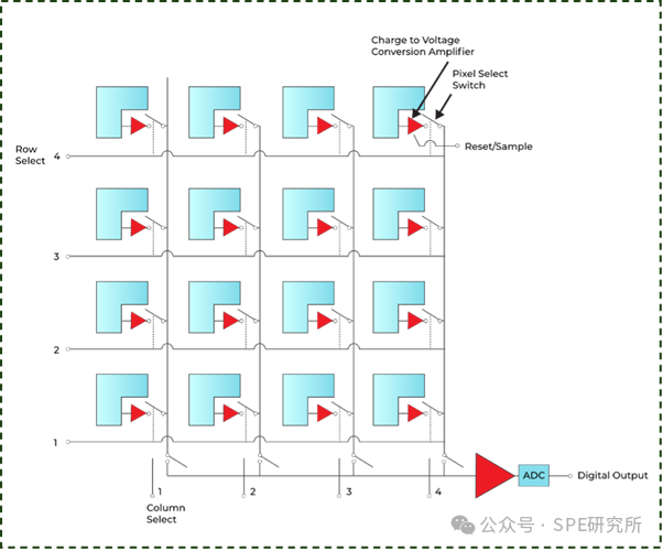
When strong light causes pixel charge saturation, the discharge channel releases excess charge to avoid overflow.
At the same time, the photoelectric signal in CMOS is directly converted into voltage within the pixel, without relying on charge transfer like CCD, thus avoiding overflow.
05 Conclusion
Let’s summarize briefly.
Highlight overflow causes distortion and significantly affects shooting results.
Horizontal overflow Blooming causes electrons to overflow to adjacent pixels.
Vertical overflow Smear manifests as vertical bright bands across the entire image.
Avoiding overexposure is key, and structural design can be optimized.
These phenomena commonly occur in CCDs, while CMOS has avoided them.
That’s all for today.
About Me
This public account is a certified photography account, but it also covers programming, photography, and the geek world.
The author is an ordinary poor person who loves various technologies and is also interested in various interesting gadgets and cats.
Talking about photography and cats, occasionally rambling about other topics.
Technology, programming, and landscape photos will be shared as they come.
If you are interested in my articles, please follow.
And don’t hesitate to like and appreciate, thank you!!