In embedded systems, on-board communication interfaces refer to the communication pathways or buses used to connect various integrated circuits with other peripheral devices. The following content summarizes commonly used on-board communication interfaces: including I2C, SPI, UART, and 1-Wire:
I2C Bus
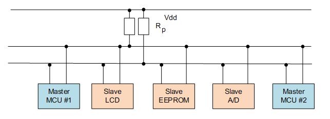
The I2C bus is a synchronous, bidirectional, half-duplex two-wire serial interface bus. Here, half-duplex means that at any given time, communication can only occur in one direction. The I2C bus was first developed and introduced by Philips Semiconductor in the 1980s. The initial design goal of I2C was to provide a simple method for connecting microprocessor/microcontroller systems with peripheral chips in televisions. The I2C bus consists of two lines: the serial clock line SCL and the serial data line SDA. The SCL line is responsible for generating synchronous clock pulses, while the SDA line is responsible for transmitting serial data between devices. The I2C bus is a shared bus system, allowing multiple I2C devices to be connected to it. Devices connected to the I2C bus can act as either master or slave devices. The master device controls the communication by initializing/terminating data transfers and generating the required synchronous clock pulses. The slave device waits for commands from the master and responds to command receptions. Both master and slave devices can act as sending or receiving devices. Regardless of whether the master device is sending or receiving, the synchronous clock signal can only be generated by the master device. The I2C protocol supports the simultaneous presence of multiple master devices on the same bus. Figure 1-1 shows the connection relationship between master and slave devices on the I2C bus.
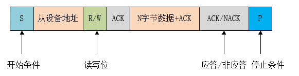 When the bus is idle, both SDA and SCL are in a high state. When the master wants to communicate with a slave, it first sends a start condition, followed by the slave address and read/write control bit, and then transmits data (either sending or receiving). At the end of the data transmission, the master sends a stop condition. Each transmitted byte consists of 8 bits, with the high bit first and the low bit last.
-
Start Condition: When SCL is high, the master pulls SDA low, indicating that data transmission is about to begin.
-
Slave Address: The first byte sent by the master is the slave address, with the high 7 bits as the address and the lowest bit as the R/W read/write control bit, where 1 indicates a read operation and 0 indicates a write operation.
Generally, the slave address can be in either 7-bit or 10-bit address mode. In the case of 10-bit address mode, the first byte’s top 7 bits are a combination of 11110XX, where the last two bits (XX) are the two highest bits of the 10-bit address, and the second byte contains the remaining 8 bits of the 10-bit slave address, as shown in the following figure:
-
Acknowledge Signal: After each byte of data is transmitted, the receiver must respond with an ACK (acknowledge). When writing data, the slave sends ACK, and when reading data, the master sends ACK. When the master reads the last byte of data, it can send NACK (Not acknowledge) followed by a stop condition.
-
Data: After the slave address is sent, some commands may be sent depending on the slave, followed by data transmission, which can be sent by either the master or the slave, with each data byte being 8 bits, and there is no limit on the number of data bytes.
-
Repeated Start Condition: During a communication session, if the master needs to transmit data to different slaves or switch between read and write operations, it can send another start condition.
-
Stop Condition: When SDA is low, the master pulls SCL high and keeps it high, then pulls SDA high, indicating the end of transmission.
SPI Bus
The SPI bus is a synchronous, bidirectional, full-duplex four-wire serial interface bus, first proposed by Motorola. SPI consists of a system with “one master device + multiple slave devices.” It is important to note that as long as only one master device is active at any given time, multiple SPI master devices can exist in the system. It is commonly used for communication between EEPROM, FLASH, real-time clocks, AD converters, digital signal processors, and digital signal decoders. To achieve communication, SPI has four signal lines, which are:
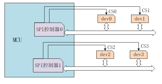 (1) Master Out Slave In (MOSI): The signal line for transmitting data from the master device to the slave device, also known as Slave Input (SI/SDI). (2) Master In Slave Out (MISO): The signal line for transmitting data from the slave device to the master device, also known as Slave Output (SO/SDO). (3) Serial Clock (SCLK): The signal line for transmitting clock signals. (4) Slave Select (SS): The signal line used to select the slave device, which is active low. The usage of SPI is shown in the following diagram:The chip shown in the figure has two SPI controllers, with each SPI controller corresponding to an SPI master device, and each SPI controller can connect to multiple SPI slave devices. The slave devices mounted on the same SPI controller share three signal pins: SCK, MISO, and MOSI, but each slave device’s CS pin is independent. The master device controls the CS pin to select the slave device, which is generally active low. At any time, only one CS pin on an SPI master device can be active, and the slave device connected to that active CS pin can communicate with the master device. Therefore, the SPI communication method can use a “one master, multiple slaves” structure for communication. Each device connected to the bus has a unique address, and the master device initiates data transmission and generates clock signals. The slave device is addressed by the master device, and only one master device is allowed at the same time. The clock for the slave device is provided by the master device through SCLK, while MOSI and MISO complete data transmission based on this pulse. The working timing mode of SPI is determined by the phase relationship between CPOL (Clock Polarity) and CPHA (Clock Phase). CPOL indicates the initial level state of the clock signal, where CPOL=0 indicates that the clock signal’s initial state is low, and CPOL=1 indicates that the initial level of the clock signal is high. CPHA indicates at which clock edge data is sampled; CPHA=0 indicates sampling data on the first clock edge, while CPHA=1 indicates sampling data on the second clock edge. There are four working timing modes based on different combinations of CPOL and CPHA: CPOL=0, CPHA=0; CPOL=0, CPHA=1; CPOL=1, CPHA=0; CPOL=1, CPHA=1.
UART
UART—Universal Asynchronous Receiver-Transmitter, as an asynchronous serial communication protocol, works by transmitting each character of data one bit at a time. It is a frequently used data bus in application development. UART-based data transmission is asynchronous serial data transmission. Serial data transmission based on UART does not require a clock signal to synchronize the transmitting and receiving ends but relies on predefined configurations between the sending and receiving devices. For both the sending and receiving devices, the serial communication configurations (baud rate, number of bits per unit word, parity, start and stop bits, flow control) must be set to be exactly the same. By inserting specific bit sequences into the data stream, the start and end of communication can be indicated. When sending a byte of data, a start bit is added at the beginning of the bit stream, and a stop bit is added at the end of the bit stream. The least significant bit of the data byte follows immediately after the start bit. The characteristics of UART serial ports are that data is transmitted one bit at a time in sequence, and only two transmission lines are needed to achieve bidirectional communication, with one line sending data while the other line receives data. UART serial communication has several important parameters, including baud rate, start bit, data bits, stop bits, and parity bit. For two ports using UART serial communication, these parameters must match; otherwise, communication will fail.
- Start Bit: Indicates the beginning of data transmission, with a logic level of “0”.
- Data Bits: Possible values are 5, 6, 7, 8, or 9, indicating the number of bits of data being transmitted. The common value is 8, as an ASCII character value is 8 bits.
- Parity Bit: Used by the receiver to check the received data, with the number of “1” bits being even (even parity) or odd (odd parity) to verify the correctness of data transmission. This bit can be omitted when used.
- Stop Bit: Indicates the end of a data frame, with a logic level of “1”.
- Baud Rate: The rate of serial communication, represented by the number of valid bits (bit) transmitted per unit time, measured in bits per second (bps). Common baud rate values include 4800, 9600, 14400, 38400, 115200, etc. The higher the value, the faster the data transmission; a baud rate of 115200 means transmitting 115200 bits of data per second.
1-Wire Interface
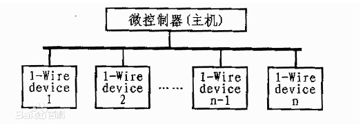
The 1-Wire interface is an asynchronous half-duplex communication protocol developed by Maxim Dallas Semiconductor (homepage: http://www.maxim-ic.com), also known as the Dallas 1-Wire® protocol. In this protocol, communication is achieved using a single signal line DQ according to the master-slave communication model. An important feature of the 1-Wire bus is that it allows energy to be transmitted over the signal line. The 1-Wire interface supports the connection of a single master device and one or more slave devices on the bus.
Parallel Interface
The on-board parallel interface is typically used for communication between the system and peripheral devices, where the peripheral devices are memory-mapped to the system’s main control unit. As long as the embedded system’s main control processor/controller has a parallel bus, devices that support the parallel bus can be directly connected to this bus system. There is a control signal interface between the peripheral devices and the main control unit, which can control data communication on the parallel bus. Here, the control signals for communication include read/write signals and device select signals. Generally, peripheral devices have a device select line; only when the main control processor enables this line is the device valid. The direction of data transmission can be from the main control unit to the peripheral device or from the peripheral device to the main control unit; this is controlled through the read and write control signal lines. Only the main control processor can control the read control signal and write control signal. Generally, peripheral devices are memory-mapped to the main control processor, allowing access to the allocated address range. At this point, the device needs to use address decoding circuits to generate chip select signals. When the address selected by the processor is within the device’s specified range, the decoding circuit triggers the chip select line, activating the device. The processor can then enable the corresponding control lines (RD and WD) to read data from the device or write data to the device. To achieve parallel communication, the system must strictly adhere to timing specifications. As mentioned earlier, parallel communication is initiated by the main control processor. If a peripheral device wants to initialize communication, it can send an interrupt to the processor to inform it of the relevant information. To achieve this functionality, the device’s interrupt line needs to be connected to the processor’s interrupt line, and the main control processor needs to trigger the corresponding interrupt. It should be noted that the width of the data bus of the main control processor determines the width of the parallel interface, which can be 4, 8, 16, 32, or 64 bits, etc. The bus width supported by the device should match exactly with that of the main control processor.
Author: IriczhaoOriginal: https://www.cnblogs.com/iriczhao/p/10816426.html
-END-| Article compiled for the dissemination of related technologies, copyright belongs to the original author |If there is any infringement, please contact for deletion |
Collection of previous good articles
Dry goods | How to learn embedded Linux well? Detailed application of state machine thinking in embedded development Hot discussion on Zhihu: Is C++ useful in embedded development?
Finally
If you find the article good,forward and share, it is also our motivation to continue updating.
5T resource giveaway!Including but not limited to:C/C++, Linux, Python, Java, PHP, artificial intelligence, PCB, FPGA, DSP, LabVIEW, microcontrollers, etc.!
Reply “more resources” in the public account to get it for free, looking forward to your attention~