Inductive components and capacitive components are both energy storage elements, with capacitors storing energy in the form of voltage (the energy stored in a capacitor at any moment is (1/2)CUc22), while inductive components store magnetic energy, represented in the form of current (the energy stored in an inductor at any moment is (1/2)LiL22). Since energy cannot change instantaneously, dynamic circuits formed by inductive components also exhibit a transitional process.
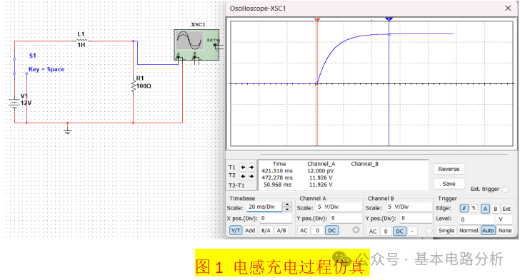
In the Multisim workspace, place 1 ideal voltage source of 12V, 1 single-pole double-throw switch S1, 1 100Ω resistor R1, and 1 1H inductor L1, along with 1 ground symbol, and then place 1 virtual oscilloscope XSC1, connecting them as shown in the diagram. From the circuit parameters, the time constant τ of this circuit can be determined as τ = L1/R1 = 1H/100Ω = 10ms, and the time required for the transitional process is 3τ – 5τ, which is 30ms – 50ms. Since the current waveform on the inductor cannot be directly observed, we will instead observe the voltage waveform across the resistor R1 (u = iR).
(1) Start the simulation, press the space bar on the keyboard or left-click on S1, to connect S1 to the right side connected to ground, discharging the inductor L1 so that the current through the inductor is 0; after starting the simulation for 421.310ms (this time can be adjusted), left-click on S1, connecting S1 to the left side connected to V1, and observe the oscilloscope waveform as shown in Figure 1. The red indicator line 1 shows a time of 421.310ms, with a magnitude of 12.000pV (approximately equal to 0V, indicating that the current at this time is approximately 0A), while the blue indicator line 2 shows a time of 472.278ms, with a magnitude of 11.926V (approximately equal to 12V, indicating that the current at this time is approximately 0.12A, making the inductor behave like a short circuit). The time difference between the two indicator lines is approximately 50ms, indicating that the current through the inductor L1 takes about 50ms to charge from 0A to 0.12A, which is consistent with theoretical calculations.
(2) The circuit structure is the same as in Figure 1, start the simulation, press the space bar on the keyboard or left-click on S1, to connect S1 to the left side connected to V1, charging the inductor L1 to 0.12A, after starting the simulation for 245.816ms (this time can be adjusted), left-click on S1, connecting S1 to the right side connected to ground, and observe the oscilloscope waveform as shown in Figure 2. The red indicator line 1 shows a time of 245.816ms, with a magnitude of 12V (indicating that the current through the inductor is 0.12A), while the blue indicator line 2 shows a time of 296.784ms, with a magnitude of 74.719mV (approximately equal to 0V, indicating that the current through the inductor is approximately 0A). The time difference between the two indicator lines is approximately 50ms, indicating that the current through the inductor L1 takes about 50ms to discharge from 0.12A to 0A, which is almost consistent with theoretical calculations.
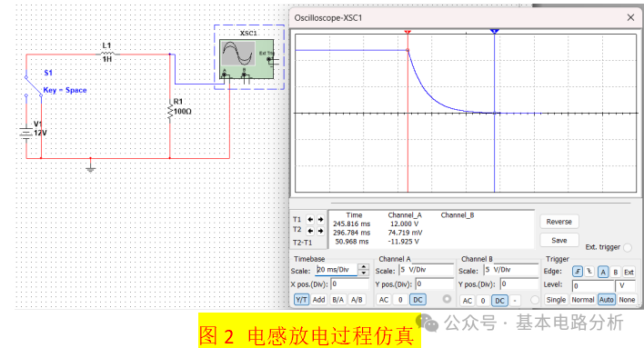 From the simulation results, it can be seen that both capacitors and inductors, as energy storage elements, exhibit transitional processes when the circuit is switched. The time constant for the capacitor charging and discharging circuit is RC, while the time constant for the inductor charging and discharging circuit is L/R. Moreover, the above simulations involve a single energy storage element in series with a resistor. If encountering circuits with one energy storage element, multiple resistors, multiple independent sources, or controlled sources, the energy storage element can be treated as the branch to be analyzed, while the remaining branches can be equivalent to an actual voltage source model using Thevenin’s theorem to analyze the charging and discharging process.