The EE History Class series has not been opened for a long time. Recently, Chips and Cheese updated their tests on the Snapdragon 820: we had also planned to trace back the topic of Snapdragon 820 mobile chip articles two years ago, but we had to shelve it due to the lack of satisfactory materials. Now, with the detailed test data from Chips and Cheese, let’s directly discuss this mobile SoC from the past.

The Snapdragon 820 is special for two main reasons. Firstly, this SoC’s CPU section uses Qualcomm’s self-developed Kryo cores instead of Arm’s public version—Qualcomm has a tradition of self-developing CPUs during the 32-bit era. The earliest Scorpion and later Krait architectures created differentiation in the mobile chip market.
After Apple’s A7 brought the iOS ecosystem into the 64-bit era, Qualcomm quickly introduced 64-bit to the Android ecosystem by hastily releasing what may be the most unwillingly mentioned product in the company’s history, the Snapdragon 810. Regardless of the actual performance of the Snapdragon 810, its various aspects appeared to be very rushed, especially since the CPU did not adopt a self-developed architecture but instead used Arm’s CPU IP—this was very un-Qualcomm.
This left the Snapdragon 810’s successor, the Snapdragon 820, with enormous expectations from the market. Qualcomm indeed returned to a self-developed architecture for the CPU section of the Snapdragon 820. However, at the same time, the Snapdragon 820 also became, to date, the last generation of Qualcomm’s self-developed CPU architecture mobile SoC chip. The subsequent Snapdragon 835 and the mobile AP SoCs that continue to this day, while still using the Kryo brand, are essentially based on the Arm Cortex-A/X series, which we refer to as the Arm public version.
Secondly, the reputation of the Snapdragon 820 seems to be in a kind of Schrödinger’s cat-like mysterious state. One of the responsibilities of the Snapdragon 820 was to dispel the shadow of the previous Snapdragon 810 and reclaim the territory lost to competitors during this period. At the beginning of its release, this chip did indeed live up to expectations, showing significant improvements in tests like Geekbench 3; it also mostly received praise from the media.
However, after a large number of Snapdragon 820 phones were released, it faced another wave of criticism. This seemed to be triggered by the release of the new testing software Geekbench 4—this chart comes from XDA-Developer. In the Geekbench 3 benchmark test, the Snapdragon 820’s single-core performance was far ahead of all competitors, including the then-popular Samsung Exynos 8890 and HiSilicon Kirin 950. But with the launch of Geekbench 4, its test scores suddenly lagged behind its competitors.
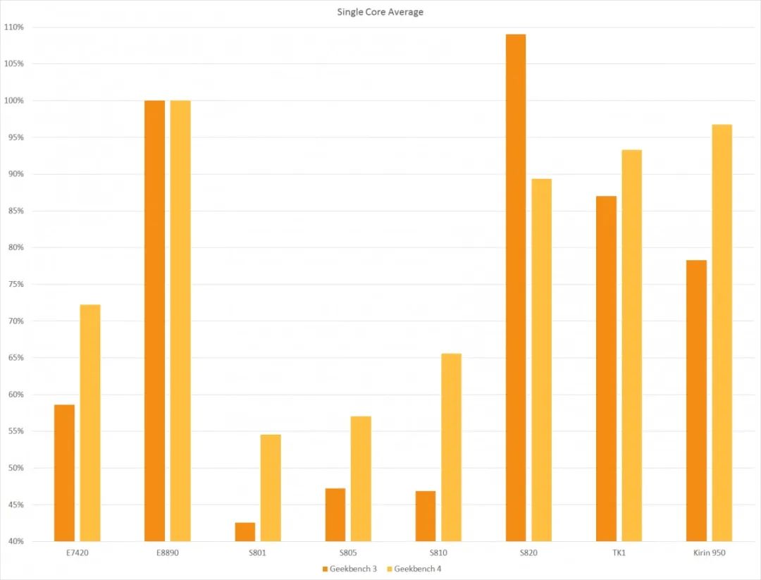
Source: XDA Developer
At the same time, there were incessant complaints about the Snapdragon 820’s poor battery life and severe heating issues, with some even placing the Snapdragon 820 alongside the Snapdragon 810 in terms of “historical status.” On the other hand, however, many new legends emerged about the Snapdragon 820 later on, including its outstanding floating-point performance—AnandTech even mentioned the Snapdragon 820’s leading scores in some test categories during their review of the Apple A12 (3-4 years later).
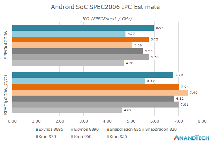
Source: AnandTech
This chart lists the IPC scores obtained from SPEC2006 testing (score ÷ frequency), in the FP floating-point test, the Snapdragon 820 surpassed all Android mobile SoCs of its time and even the Snapdragon 845 two years later. There’s also the comparison of single-core floating-point performance IPC from Geekbench 4:
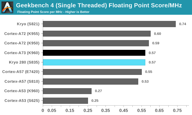
Source: AnandTech
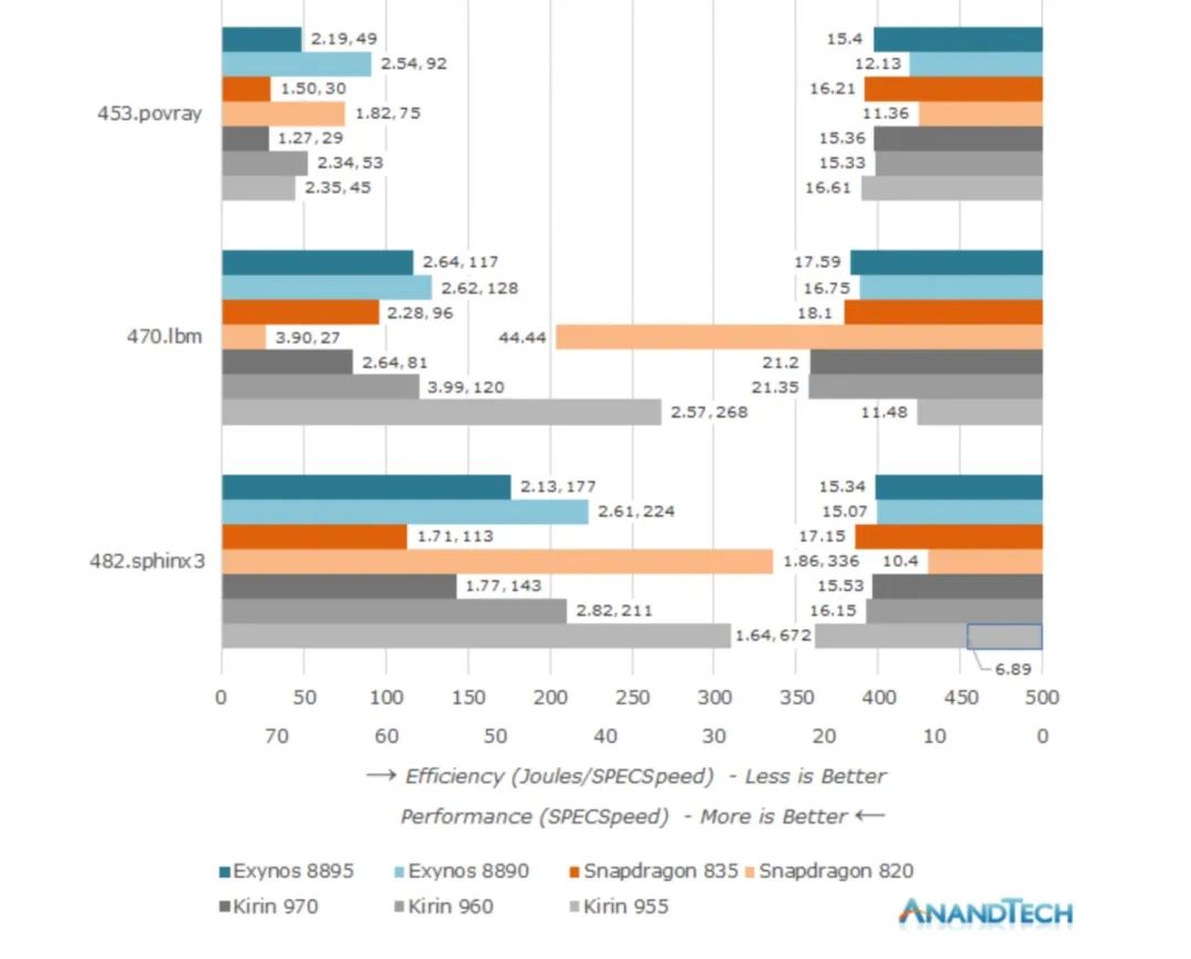
The following chart excerpts some sub-items from the SPEC2006 test, showing the Snapdragon 820’s “extraordinary” specialization—such as in the 470.lbm test where its performance and efficiency were astounding; while in the 482.sphinx3 test, the results were quite tragic… (The left bar reflects efficiency, shorter is better; the right bar reflects performance, longer is better.)
In this EE history class, we will use the tests from Chips and Cheese to discuss the Snapdragon 820 released in 2015. Perhaps based on this analysis, we can glimpse why the Snapdragon 820 became Qualcomm’s last generation of self-developed CPU architecture chip.
Reviewing Snapdragon 820
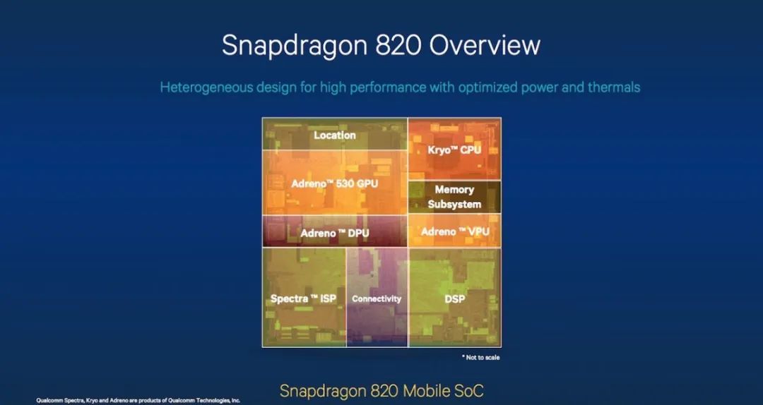
It has been quite some time, so let’s review some basic configuration information of the Snapdragon 820 and its contemporaneous iteration, the Snapdragon 821. The Snapdragon 820 chose Samsung’s 14LPP manufacturing process; the CPU features a 2 big cores, 2 small cores design, with both big and small cores being Kryo architecture, differing in frequency and cache sizes; the GPU is Adreno 530; DSP Hexagon 680; supports LPDDR4 1333/1866; modem X12 LTE;
We will mainly focus on the CPU section of the Snapdragon 820/821, and won’t delve into peripheral information such as GPU, DSP, memory, and I/O support.
 Unlike Arm’s big.LITTLE design, Qualcomm’s Snapdragon 820 has both types of cores using the same Kryo microarchitecture—only the big cores are allocated higher frequencies and larger cache sizes. Historical data from Wikipedia shows that the big core frequency of the Snapdragon 820 (MSM8996) is 2.15GHz, while the small core frequency is 1.59GHz; the later released Snapdragon 821 had slightly higher frequencies, especially with a version of the small core having a frequency of 2.19GHz.
It is worth mentioning that the Snapdragon 820 did not come with L3 cache. In fact, the contemporary Arm Cortex-A72 also lacked L3 cache, but there were rumors that the Snapdragon 820 would feature L3 cache. AnandTech even mentioned that based on Qualcomm’s information regarding the cache block, there should be L3 cache, but when the Snapdragon 820 was officially released, L3 cache was still not seen.
From AnandTech’s Geekbench 3 and SPEC2000 test results for the Snapdragon 820 in 2015, the Snapdragon 820 showed significant improvements compared to the Snapdragon 810, or rather, the Qualcomm Kryo architecture had advantages over the Arm Cortex-A57. However, some sub-items of the SPEC2000 showed a significant decline in performance, which was somewhat puzzling; AnandTech mentioned that the compiler configuration was not yet optimized.
It should be noted that contemporaneous mobile chips to the Snapdragon 820 include the Apple A9, HiSilicon Kirin 950, and Samsung Exynos 8890. As mentioned earlier, after the release of Geekbench 4, the Snapdragon 820’s testing lead among contemporaneous competitors was reversed. One theory is that Geekbench 4 significantly lowered the weight of floating-point performance in its tests—this point we cannot verify, as the official documentation for Geekbench 3 describes each sub-item ambiguously; this issue may be addressed later.
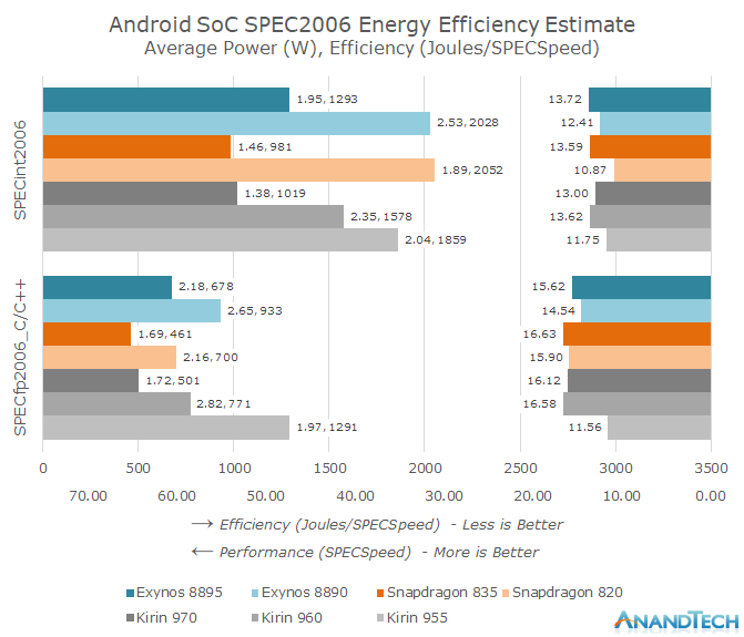
Additionally, despite the earlier IPC comparisons showing the Snapdragon 820 looking quite good, in terms of energy efficiency and overall performance dimensions (as shown in the image below), the Snapdragon 820 was a complete mess—especially under the SPECint2006 test, where it not only had the worst performance (the right bar, longer indicates better performance), but also the highest energy consumption, with the worst energy efficiency (the left bar, total energy consumption ÷ score, indicating the energy needed for each score point).
When Desktop Cores Come to Mobile
These pieces of information are still somewhat black-boxed and coarse. Chips and Cheese recently conducted a series of microbenchmarking, reverse-engineering more microarchitecture information of this generation’s CPU section. They tested an LG G6 phone with a Snapdragon 821, but fortunately, the differences between the 821 and 820 are minimal, and the microarchitecture remains unchanged, which can still illustrate the issues.
However, before delving into microarchitecture, let’s first look at the most intuitive and straightforward aspects. In the further analysis of microarchitecture later on, we will see that the Snapdragon 820’s Kryo architecture, in terms of scale, is quite large for mobile chips in 2016, including a front end with a 4-wide width, excellent scheduler layout in the execution engine section, low-latency L1-D, and ample integer execution unit resources, achieving high IPC scores.
Additionally, there is strong branch handling capability and a large reorder buffer capacity for branch handling; the load/store unit employs sophisticated logic to handle storage forwarding—some situations even Arm’s contemporary architectures cannot handle. Chips and Cheese evaluated Kryo as a desktop core with reduced frequency—although we believe calling it a “desktop core” is somewhat exaggerated.
However, the Android ecosystem at that time did not have designs that could match its core bandwidth, execution resources, or reorder queue capacity; such scale was only achieved by Android mobile AP SoCs many years later. But this may have also been a key factor in the demise of Kryo and even Qualcomm’s self-developed CPU architectures at that time.
Moreover, Qualcomm did not have a small core solution like Arm’s at that time, so the “big.LITTLE” design of the Snapdragon 820 actually stacked the same type of core, meaning the “small core” of the Snapdragon 820 was not small at all—hence the Snapdragon 820’s CPU only had 4 cores; compared to the common 8-core solutions of Arm’s public version at that time, this naturally affected multi-threading performance.
Was this oversized core design really suitable for the Android ecosystem of that time (although it seems “desktop-level” was already the message Apple was conveying during the A7 chip era)?
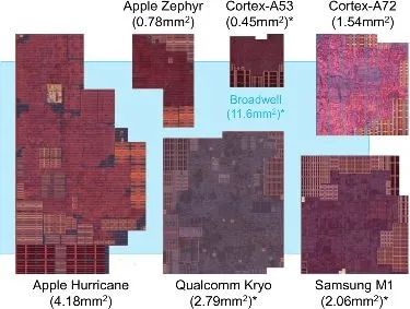
The Kryo core was likely the largest core in mobile chips at that time, aside from Apple (though it cannot compare to Broadwell). So why did Apple succeed, but Qualcomm’s Snapdragon 820 did not, and why did they abandon such a strategy later? From a market perspective, we should first consider that the larger area led to higher costs—which would definitely not be what Qualcomm wanted to see. After all, Apple not only designs chips but also sells phones; this is completely different from Qualcomm’s business model.
But aside from that, there seem to be more specific technical issues at the execution level.
Kryo Core: A Very Wide Front End
The following image is a block diagram of the Snapdragon 820/821’s Kryo architecture obtained through reverse engineering, although some information remains uncertain.
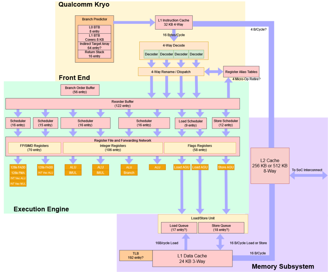
Source: Chips and Cheese
Regarding the front-end branch prediction, Chips and Cheese rated it well for its branch prediction capabilities, able to recognize patterns similar to Cortex-A72, but when there are many branches, its performance is not that great, and it still lags behind desktop-level Skylake.
In terms of branch target cache (branch target caching), it is relatively “conservative” (possibly opting for a fast branch address calculator and an L0+L1 instruction cache scheme, with an 8KB L0 cache and a 2-cycle delay). Kryo performs better than A72 in this regard. Cortex-A72’s use of a BTB (branch target buffer) is slower than Kryo’s L0 reading and target address calculation.
However, exceeding 8KB incurs a penalty in latency, but it remains within expected limits. The indirect branch prediction situation is basically similar; Cortex-A72 chooses a deeper return stack, while Kryo opts for a 16-entry return stack for return-type predictions.
Moving to the instruction fetch section, Kryo uses a 32KB L1-I (L1 instruction cache); Kryo can read and decode up to 4 instructions per cycle, thus being termed 4-wide. Purely in terms of this width, Kryo can be considered a relatively wide mobile CPU architecture. Cortex-A72 has a front end of 3-wide, while A73 shrank to 2-wide—at least in the mobile field at that time, Kryo could be considered super-wide, which seems to be a tradition of Qualcomm’s self-developed CPU architectures.
However, it is worth noting that while Cortex-A72’s front end is 3-wide, it comes with a 48KB L1-I (the previous generation Cortex-A57 also had 48KB); Kryo only has 32KB in this regard. When fetching code from L2, the front end’s throughput can drop sharply to 1 IPC, as illustrated in the following image showing the decline of both under different data coverage conditions. It is noteworthy that this is also a significant difference between low-power cores and desktop processor cores, as when an L1-I cache miss occurs, the front end’s throughput drops significantly; Kryo is still hard to call a “desktop” core.
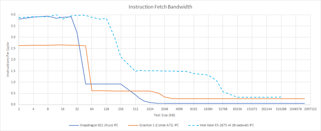
Source: Chips and Cheese
Ample Back-End Execution Resources
The out-of-order execution section of Kryo has a ROB (reorder buffer) depth similar to Cortex-A72, but there are significant differences in handling different out-of-order buffers. Especially in integer code with many branches, Kryo has a higher utilization rate, and the structure of the flag register file with larger capacity is also a feature; Cortex-A72 shows performance focused on scalar floating-point code in this area, but Kryo has full-width vector registers, so A72 has no advantage here.
Additionally, Kryo also has advantages in scheduler capacity. Chips and Cheese evaluates Kryo’s scheduler as not being fully “distributed”; the integer scheduler is made up of two 2-port queues, similar to Cortex-A72’s 4 queues in scheduling capacity, but this design is more flexible; the scheduler for floating-point/vector and storage access parts has a similar queue distribution to A72, but these queue capacities are larger than A72. Chips and Cheese believes that Kryo’s scheduler design significantly exceeds A72, but it may come at the cost of power consumption and area.
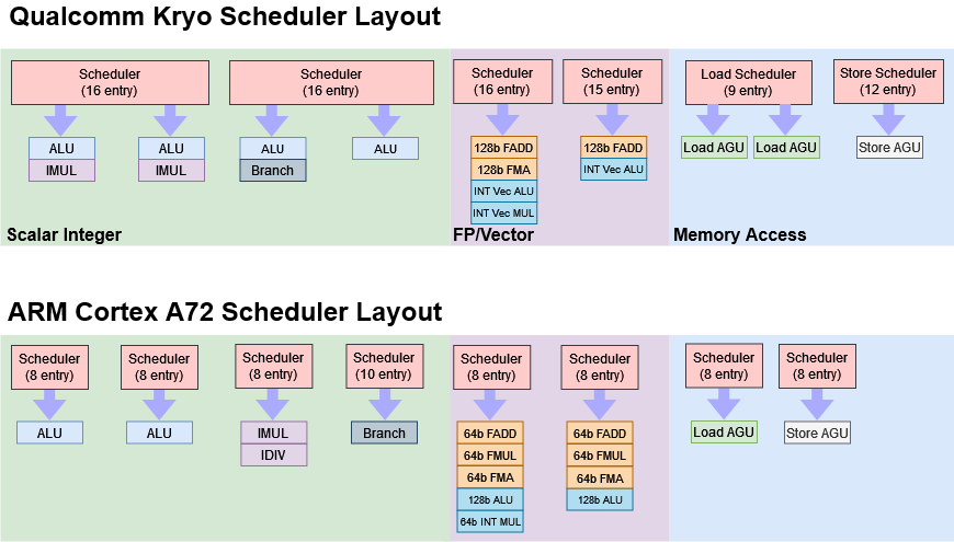
The configuration of Kryo’s integer execution units is still strong, with a throughput of 4 basic integer operations per cycle reaching desktop CPU levels, especially with outstanding integer multiplication throughput, although its branch throughput is slightly weaker than desktop cores like Skylake. Cortex-A72 has similar multiplication latency to Kryo at 5 cycles, but only has 1 port for integer multiplication; with a total of 2 ALUs, port contention can occur.
In terms of floating-point and vector execution: for scalar floating-point performance, Kryo has 2 very fast 3-cycle FP adders, while Cortex-A72 is slightly slower at 4 cycles. In terms of vector floating-point performance, Kryo theoretically has higher throughput because the 128-bit FMA (fused multiply-add) only occupies one FP floating-point pipeline—thus achieving dual-issue of one 128-bit floating-point add and one 128-bit FMA instruction, allowing for 12 floating-point operations per cycle; moreover, Kryo’s FMA latency is also controlled at 5 cycles, while Cortex-A72 takes 7 cycles to complete the same operation.
Additionally, compared to Cortex-A72, Kryo has significantly better vector integer execution capabilities. Vector INT32 addition is completed in 1 cycle, while A72 requires 3 cycles. For vector INT32 multiplication, both require 4 cycles, but do not forget that Kryo has double the throughput.
Meanwhile, Kryo can perform 2 128-bit vector load operations per cycle, although they are not contiguous; on the data write side, Kryo can complete one 128-bit store operation per cycle, while A72 requires 2 cycles.
At this point, we may partially understand some of the specialization exhibited by the Snapdragon 820 in tests.
Access and Cache Access: A Bit Tragic
This section is worth mentioning regarding Kryo’s store forwarding (occurs during write operations when reading from the same address immediately after), achieving the storage forwarding characteristics of Skylake. Chips and Cheese describes this part as quite sophisticated.
However, the forwarding latency reached 13 cycles, which is as tragic as AMD’s old Bulldozer, and one must consider that Kryo’s frequency is not high; specific data can be found in Chips and Cheese’s article. Cortex-A72 performs well in memory dependency, with forwarding typically having a latency of 7 cycles, even for the most expensive cross-cache line, A72 is still faster than Kryo.
In terms of TLB (Translation Lookaside Buffer), Kryo has a 192-entry L1 TLB, without a multi-level design—large data coverage leads to tragedy.
Next, let’s look at the performance related to cache access. As mentioned earlier, Kryo employs a two-level cache design. Chips and Cheese’s data shows that the L1-D (level 1 data cache) capacity is only 24KB, with an access latency of 3 cycles (AnandTech’s data is 32KB L1-D);
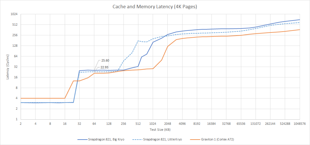
Source: Chips and Cheese
The L2 cache is one for each cluster of big and small cores, specifically for the tested Snapdragon 821 big core cluster, it has a 768KB L2 cache with a latency of 25 cycles; the small core cluster has 512KB with 23 cycles. This data differs from what AnandTech initially reported, which suggested that the big core cluster’s L2 cache could be 1MB (for the Snapdragon 820). However, both parties cannot confirm the accuracy of the data.
Regardless, Kryo’s L2 cache latency appears to be very high, and the capacity is also small. In terms of concrete time, Kryo’s L2 cache latency reached 10.9ns, which is roughly on par with the much larger L3 cache of Intel Skylake—of course, the latter’s frequency is much higher. According to tests of Amazon’s Graviton 1 processor, Cortex-A72 accesses a shared 1MB L2 cache in 21 cycles, achieving faster speed and larger capacity.

From a bandwidth perspective, Kryo and A72 are both around 8 bytes per cycle. However, Kryo’s more dispersed L2 design has advantages in bandwidth under increasing thread counts. However, given the small capacity, it may not have much practical effect.
Some Speculations on the Snapdragon 820‘s Reputation Reversal
The entire storage subsystem of the Snapdragon 820 CPU appears to be completely mismatched with the quality of its core components. A few years ago, some boldly speculated that the original design of the Snapdragon 820 might indeed have featured L3 cache (consistent with AnandTech’s earlier statement); additionally, it was speculated that Qualcomm might have cut back on L1 cache after discovering that the Snapdragon 820’s power consumption was not as expected, since even the Snapdragon 810’s A57 had 48KB L1-I + 32KB L1-D.
Upon careful consideration, if this set of configurations had included L3 cache and increased L1 cache capacity, it would have made Kryo appear much more coordinated overall.
Regarding the reversal of the Snapdragon 820’s performance between Geekbench 3 and Geekbench 4, it is likely indeed related to the adjustment of floating-point performance scoring weights in Geekbench 4; on the other hand, it may also be significantly associated with the L1 cache cut and the inadequacy of L2 cache—Linus Torvalds previously criticized Geekbench 3, stating “Geekbench is SH*T,” and that they are “mainly small kernels,” doubting that most of the test code “code footprint basically fits in an L1-I cache.”
In other words, much of the test code for Geekbench 3 was directly placed into L1, which conveniently concealed the Snapdragon 820 CPU’s weak performance in the storage subsystem.
One more point worth mentioning is that the Snapdragon 820 and 821 actually have at least 4 different model versions, each with varying frequencies. This may indicate issues with yield control during chip manufacturing—there’s a high probability that the Snapdragon 820’s final PPA performance, after passing through Samsung foundry, was indeed beyond Qualcomm’s expectations, necessitating relatively rushed adjustments.
Chip and Cheese summarized that the Snapdragon 820’s cache system is awkward, with both small and slow L2 cache failing to adequately feed the execution engine. Kryo itself also has problems; even though the load/store data dependency handling mechanism is advanced, the data forwarding is extremely slow; with only a single-level TLB design, exceeding 768KB leads to page walk penalties of over 28 cycles…
In fact, a few improvements to the cache configuration would significantly enhance the overall performance of the Snapdragon 820; adding a second-level TLB and rectifying the high latency of data forwarding would also improve the situation. Additionally, Chips and Cheese believes that if the Kryo architecture could employ a more advanced manufacturing process, the outcomes might be much more ideal—not only reducing power consumption and heat generation but also increasing the core count.
Finally, it is worth mentioning that we know Qualcomm acquired Nuvia in 2021; at the same time, Arm has been tightening its licensing strategy; both sides are still in conflict. Therefore, Qualcomm’s path of self-developed CPUs is likely to continue, meaning the Snapdragon 820 will not be the last mobile chip utilizing Qualcomm’s self-developed CPU, even though there are still many variables involved.
In fact, the abandonment of self-developed CPU solutions by Qualcomm back then was largely related to the increasingly mature trend of Arm’s public designs. Moreover, at that time, Arm officially launched the Built on Arm Cortex Technology licensing method, and the Snapdragon 835 was based on this BoC license, semi-customizing the Cortex-A73. Therefore, Qualcomm’s direction may also be significantly influenced by Arm’s strategies.
Exciting Content from Video Channel
👇