Click the “Turing AI” above and select “Star” public account
The AI knowledge you want will be delivered to you in no time


Source: Everyone is a Geek
The CPU is the core component of modern computers, also known as the “microprocessor”. For PCs, the specifications and frequency of the CPU are often used as important indicators to measure a computer’s performance. The Intel x86 architecture has been around for over twenty years, and the x86 architecture CPU has a profound impact on the work and lives of most of us.
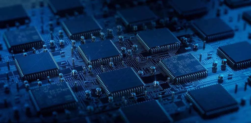
Many friends who have a little knowledge of computers will know that the most important thing inside the CPU is the transistor. To improve the speed of the CPU, the most important point is simply how to fit more transistors into the same CPU area. Since the CPU is so small and precise, it contains a considerable number of transistors, so it is absolutely impossible to complete by hand and can only be processed through photolithography technology.
This is why a CPU can contain such a large number of transistors. A transistor is essentially a binary switch: on and off. If you recall the era of basic computing, that was everything a computer needed to work. The two choices, on and off, correspond to 0 and 1 for machines. So how do you make a CPU? In today’s article, we will tell you step by step how to go from a pile of sand to a powerful integrated circuit chip.
The Basic Raw Materials for CPU Manufacturing
If you ask what the raw materials for a CPU are, everyone can easily answer—silicon. This is true, but where does silicon come from? It actually comes from the most inconspicuous sand. It’s hard to imagine that a CPU, which is expensive, complex in structure, powerful, and full of mystery, actually comes from that worthless sand. Of course, there must be a complex manufacturing process in between. However, it is not just about grabbing a handful of sand as raw material; it must be selected carefully to extract the purest silicon raw material. Just imagine, if a CPU is made from the cheapest and most abundant raw materials, what would the quality of the finished product be like? Could you still use a high-performance processor like today?
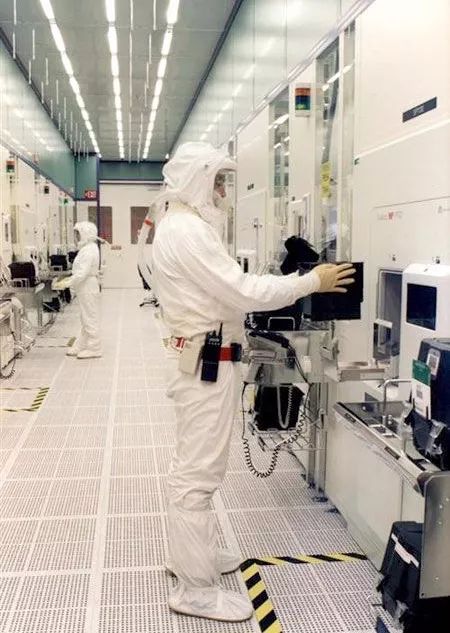
Besides silicon, another important material needed to manufacture CPUs is metal. So far, aluminum has become the main metal material for making internal components of processors, while copper is gradually being phased out for some reasons. Under the current operating voltage of CPUs, the electrical migration characteristics of aluminum are significantly better than those of copper. The so-called electromigration problem refers to the phenomenon where a large amount of electron flow passes through a conductor, causing the atomic structure of the conductor to be displaced by electron collisions, leaving vacancies. Too many vacancies can lead to the disconnection of conductive connections, and displaced atoms can cause short circuits elsewhere, affecting the logical functions of the chip and rendering it unusable.
In addition to these two main materials, some types of chemical raw materials are also needed during the chip design process, which play different roles, but will not be elaborated here.
The Preparation Phase of CPU Manufacturing
After the collection of essential raw materials is completed, some of these raw materials need to undergo some preprocessing work. As the main raw material, the processing of silicon is crucial. First, silicon raw materials need to undergo chemical purification, which brings them to the level suitable for semiconductor industry use. In order for these silicon raw materials to meet the processing needs of integrated circuit manufacturing, they must also be shaped. This step is accomplished by melting the silicon raw material and then injecting the liquid silicon into a large high-temperature quartz container.
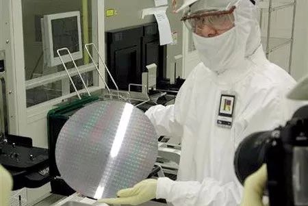
Then, the raw materials are melted at high temperatures. In middle school chemistry classes, we learned that many solids have a crystalline structure, and silicon is no exception. To meet the requirements for high-performance processors, the entire silicon raw material must be highly pure, i.e., single-crystal silicon. Then, using a rotating stretching method, the silicon raw material is extracted from the high-temperature container, resulting in a cylindrical silicon ingot. Currently, the diameter of the silicon ingot’s circular cross-section is 200 mm.
However, Intel and some other companies have already started using silicon ingots with a diameter of 300 mm. Increasing the cross-sectional area while maintaining the various characteristics of the silicon ingot is quite challenging, but as long as companies are willing to invest a large amount of money in research, it can still be achieved. Intel’s factory for developing and producing 300 mm silicon ingots cost about $3.5 billion, and the success of this new technology allows Intel to manufacture integrated circuit chips with higher complexity and stronger functionality. The factory for 200 mm silicon ingots also cost $1.5 billion.
After forming the silicon ingot and ensuring it is an absolute cylinder, the next step is to slice this cylindrical silicon ingot. The thinner the slices, the less material is used, and naturally, more processor chips can be produced. The slices must also undergo mirror polishing to ensure the surface is absolutely smooth, followed by checking for distortions or other issues. This quality inspection step is particularly important as it directly determines the quality of the finished CPU.
The new slices need to be doped with some substances to become true semiconductor materials, and then the transistor circuits representing various logical functions are etched onto them. The doped atomic substances enter the gaps between silicon atoms, and atomic forces act between them, giving the silicon raw material semiconductor properties. Today’s semiconductor manufacturing mostly uses CMOS technology (Complementary Metal-Oxide-Semiconductor).
Among them, the term “complementary” refers to the interaction between N-type MOS transistors and P-type MOS transistors. In electronic technology, N and P represent negative and positive, respectively. In most cases, the slices are doped with chemical substances to form a P-type substrate, and the logic circuits etched on it must follow the characteristics of nMOS circuits, which have higher space utilization and are more energy-efficient. At the same time, in most cases, the appearance of pMOS transistors must be minimized because, in the later stages of the manufacturing process, N-type materials need to be implanted into the P-type substrate, which can lead to the formation of pMOS transistors.
After the doping process is completed, the standard slice is finished. Each slice is then placed in a high-temperature furnace for heating, and by controlling the heating time, a layer of silicon dioxide film is generated on the surface of the slice. By closely monitoring the temperature, air composition, and heating time, the thickness of this silicon dioxide layer can be controlled. In Intel’s 90-nanometer manufacturing process, the width of the gate oxide has reached an astonishing 5 atomic layers. This gate circuit is also part of the transistor gate circuit, which controls the flow of electrons between them. By controlling the gate voltage, the flow of electrons is strictly regulated, regardless of the voltage levels at the input and output ports.
The final step in the preparation work is to cover a photosensitive layer on top of the silicon dioxide layer. This layer of material is used for other control applications within the same layer. This material has good photosensitivity when dry, and after the photolithography process is completed, it can be dissolved and removed by chemical methods.
Photolithography
This is currently one of the most complex steps in the CPU manufacturing process. Why is that? The photolithography process involves using light of a certain wavelength to engrave corresponding marks in the photosensitive layer, thereby changing the chemical properties of the material in that area. This technology requires strict specifications for the wavelength of light used, necessitating the use of short-wavelength ultraviolet light and large-curvature lenses. The etching process is also affected by contaminants on the wafer. Each etching step is a complex and precise process.
The amount of data required to design each step can be measured in units of 10GB, and the number of etching steps required to manufacture each processor exceeds 20 (each step involves one layer of etching). Moreover, if the blueprints for each layer of etching are enlarged significantly, they can be compared to the map of New York City and its suburbs, and may even be more complex. Just imagine shrinking the entire New York map down to an actual area size of only 100 square millimeters on a chip; the complexity of the chip’s structure is evident.
Once all these etching tasks are completed, the wafer is flipped over. Short-wavelength light shines through the engraved marks on the quartz mask onto the photosensitive layer of the wafer, and then the light and mask are removed. By using chemical methods, the exposed photosensitive layer material is removed, and silicon dioxide is immediately generated below the engraved areas.
Doping
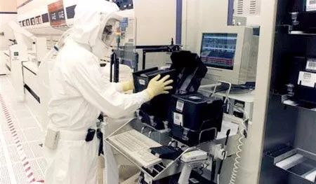
After the remaining photosensitive layer material is removed, what remains is the silicon layer exposed beneath the silicon dioxide layer, which is now filled with grooves. After this step, another silicon dioxide layer is completed. Then, another polysilicon layer with a photosensitive layer is added. Polysilicon is another type of gate circuit. Since metal materials are used here (hence the term metal-oxide-semiconductor), polysilicon allows for the establishment of gate circuits before the voltage at the transistor queue ports takes effect. The photosensitive layer must also be etched through a mask using short-wavelength light. After another etching, the required gate circuits are basically formed. Then, the exposed silicon layer is subjected to ion bombardment through chemical means, which aims to generate N-channel or P-channel. This doping process creates all the transistors and their interconnections, with each transistor having an input and output, referred to as ports.
Repeating This Process
From this step onward, you will continue to add layers, adding a silicon dioxide layer and then photolithographing once. Repeat these steps, and a multi-layer three-dimensional structure appears, which is the embryonic state of the processor you are currently using. Metal coating technology is used for interlayer conductive connections. Today’s P4 processors use 7 layers of metal connections, while Athlon64 uses 9 layers. The number of layers used depends on the initial layout design and does not directly represent differences in the performance of the final product.
Testing and Packaging Process
The next few weeks require the wafer to undergo a series of tests, including checking the electrical properties of the wafer and identifying any logical errors, and if so, determining at which layer they occur. Subsequently, each defective chip unit on the wafer will be tested individually to determine if special processing is needed for that chip.
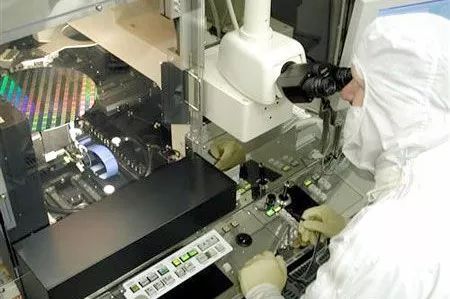
Then, the entire wafer is cut into individual processor chip units. In the initial tests, those units that failed to meet the standards will be discarded. These cut chip units will be packaged in some way so that they can be smoothly inserted into a motherboard with a specific interface specification. Most Intel and AMD processors are covered with a heat sink.
After the processor product is completed, comprehensive chip function testing is also required. This step produces different grades of products; some chips have relatively high operating frequencies, so they are labeled with high-frequency product names and numbers, while those with relatively low operating frequencies are modified and labeled with other low-frequency models. This is how processors with different market positioning come about. Some processors may have some deficiencies in chip functionality. For example, if there is a defect in the cache function (this defect is enough to cause most CPUs to fail), they will have some cache capacity disabled, reducing performance and, of course, lowering the product price, which is the origin of Celeron and Sempron.
Before the CPU is placed in the packaging box, a final test is generally conducted to ensure that the previous work is accurate. Depending on the previously determined maximum operating frequency, they are placed in different packages and sold worldwide.
After reading this, you should have a deeper understanding of the CPU manufacturing process. The manufacturing of CPUs can be said to be a culmination of cutting-edge scientific technologies from multiple fields. The CPU itself is so small that if the materials inside were separated and sold individually, they would probably not fetch much money. However, the manufacturing cost of a CPU is astonishing, which may help us understand why these things are so expensive.
In this testing phase, it is crucial. For example, whether your processor is a 6300 or a 6400 will be determined in this phase, and the 6300 is not inherently a 6300; it is only after testing that it is found that the processor cannot stably operate under the 6400 standard and can only work stably under the 6300 standard. Thus, the processor is defined, frequency locked, ID defined, packaged, and labeled as 6300.
Taking AMD as an example: processors with the same core all come off the same production line. If they can stably operate at 2.8GHz with 1M*2 cache, they are defined as 5600+. If there are defects in the cache or cutting issues in that half, it becomes 5400+. If the cache is fine but the frequency can only pass the test at 2.6G, then it is 5200+. If the cache has defects, it is cut down to become 5000+… and so on until it is tested down to 3800+. If it is still unstable, it will either be transformed into a single-core Athlon 64 or a single-core Sempron or become an ES version of the dual-core Sempron. If a batch cannot work under the 3800+ conditions but can work under the 3600+ conditions, then 3600+ will be released. If a batch can work under 3G, 1M*2 conditions, then 6000+ will be released. This explains why processors are always released first as mid-range models, while high-end and low-end models are released later. Of course, later factories may save costs by specifically opening up low-end production lines, and various low-end processors like Celeron and Sempron will be released in succession, while high-end production lines may transform individual unstable processors into low-end processors, such as cutting the Athlon 64 cache to become Sempron 64.
Intel Core i7 Production Process Illustrated
Sand: Silicon is the second most abundant element in the Earth’s crust, and the sand after deoxidation (especially quartz) contains up to 25% silicon, existing in the form of silicon dioxide (SiO2), which is the basis of the semiconductor manufacturing industry.
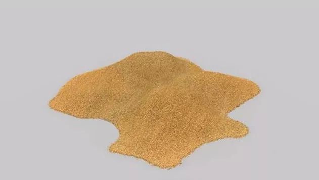
Silicon Smelting: 12-inch/300 mm wafer level, same below. Through multiple purification steps, silicon suitable for semiconductor manufacturing quality is obtained, scientifically known as electronic-grade silicon (EGS), with at most one impurity atom for every million silicon atoms. This image shows how large crystals are obtained through silicon purification smelting, resulting in a silicon ingot.
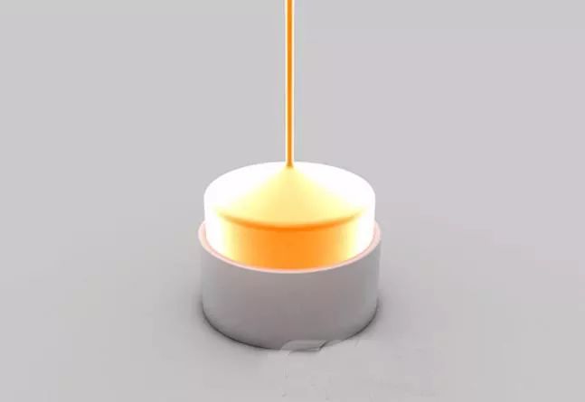
Single Crystal Silicon Ingot: The whole ingot is basically cylindrical, weighing about 100 kg, with a silicon purity of 99.9999%.
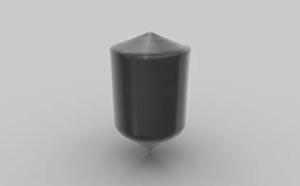
Silicon Ingot Cutting: Horizontally cut into circular individual silicon wafers, which we commonly refer to as wafers. By the way, now you know why wafers are all round, right?
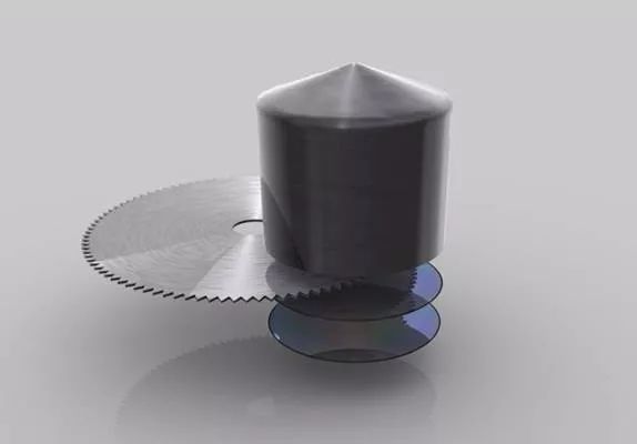
The Wafer: The cut wafer becomes almost flawless after polishing, with a surface that can even be used as a mirror. In fact, Intel does not produce these wafers itself but purchases finished products from third-party semiconductor companies and further processes them using its own production line, such as the mainstream 45nm HKMG (High-K Metal Gate). It is worth mentioning that the wafer size used by Intel at the beginning of its establishment was only 2 inches/50 mm.
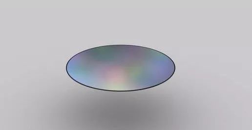
Photoresist: The blue part in the image is the photoresist liquid that is poured onto the wafer during rotation, similar to the process of making traditional film. The rotation of the wafer allows the photoresist to be spread very thin and very evenly.

Photolithography: The photoresist layer is then exposed to ultraviolet (UV) light through a mask, becoming soluble. The chemical reaction that occurs during this process is similar to the change in film when the mechanical camera shutter is pressed. The mask bears the pre-designed circuit patterns, and ultraviolet light passing through it illuminates the photoresist layer, forming the circuit patterns of the microprocessor. Generally speaking, the circuit patterns obtained on the wafer are one-quarter of the patterns on the mask.
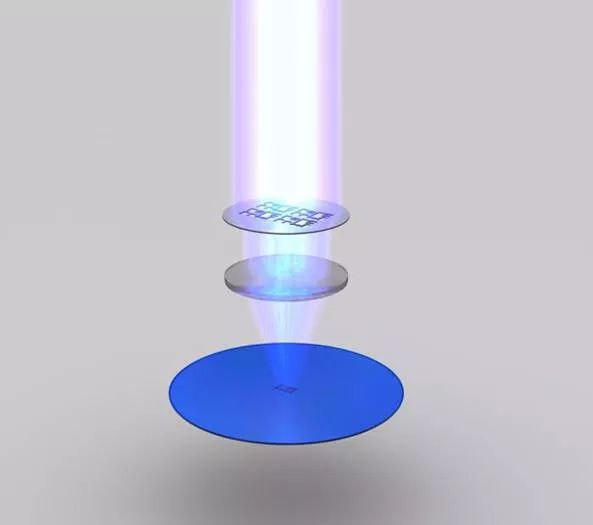
Photolithography: This leads to the transistor level of 50-200 nanometers. A single wafer can yield hundreds of processors, but from here, the focus narrows down to one of them, demonstrating how to make transistors and other components. Transistors act as switches, controlling the direction of current. Today’s transistors are so small that about 30 million can fit on the head of a pin.
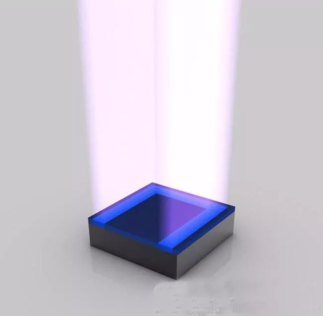
Dissolving the Photoresist: The photoresist exposed to ultraviolet light during the photolithography process is dissolved, leaving a pattern consistent with the mask.
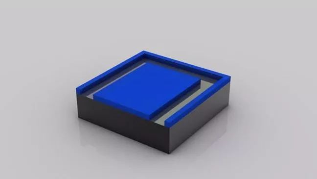
Etching: Chemical substances are used to dissolve the exposed parts of the wafer, while the remaining photoresist protects the parts that should not be etched.
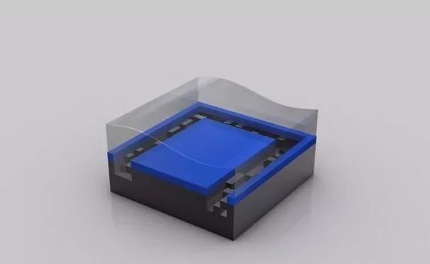
Removing the Photoresist: After the etching is completed, the mission of the photoresist is declared complete. Once removed, the designed circuit pattern can be seen.
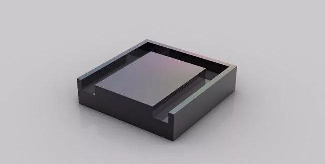
Photoresist: Apply another layer of photoresist (the blue part), then photolithograph, and wash away the exposed parts, leaving the remaining photoresist to protect the areas that will not undergo ion implantation.
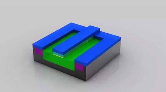
Ion Implantation: In a vacuum system, ions of doped atoms are accelerated and injected into solid materials, forming a special implanted layer in the injected area, changing the conductivity of the silicon in these areas. After being accelerated by an electric field, the speed of the injected ion flow can exceed 300,000 kilometers per hour.
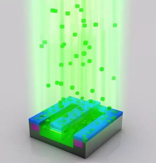
Removing the Photoresist: After ion implantation is completed, the photoresist is also removed, and the implanted area (in green) has been doped with different atoms. Note that the green area now differs from the previous one.
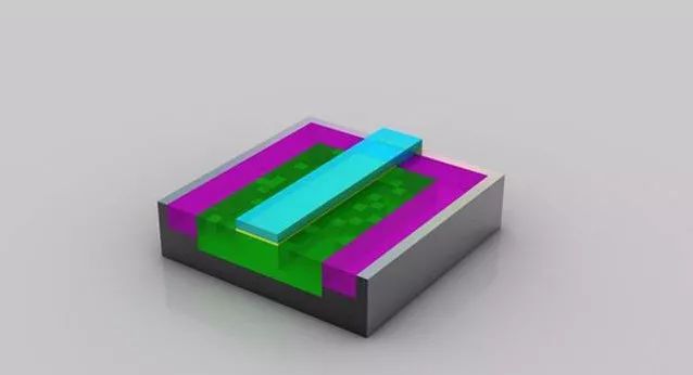
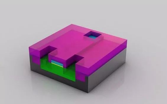
The Transistor is Ready: At this point, the transistor is basically complete. Three holes are etched into the insulating material (magenta) and filled with copper to interconnect with other transistors.
Electroplating: A layer of copper sulfate is plated onto the wafer, depositing copper ions onto the transistors. Copper ions move from the positive electrode (anode) to the negative electrode (cathode).
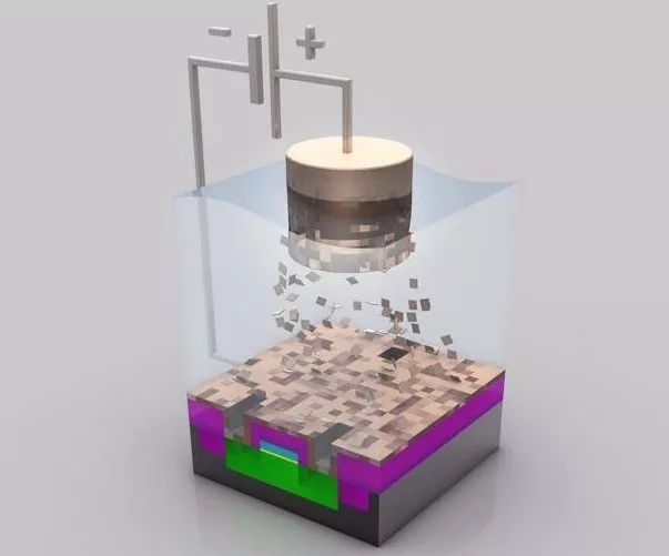
Copper Layer: After electroplating is completed, copper ions are deposited on the surface of the wafer, forming a thin layer of copper.
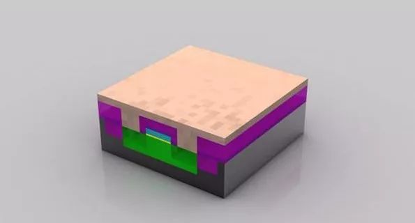
Polishing: The excess copper is polished away, smoothing the surface of the wafer.
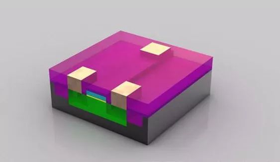
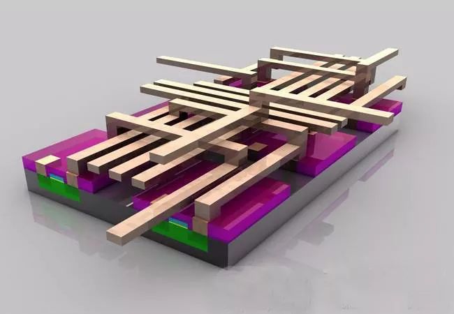
Metal Layer: At the transistor level, a combination of six transistors, approximately 500 nanometers. A composite interconnection metal layer is formed between different transistors, with the specific layout depending on the different functionalities required by the corresponding processor. The surface of the chip appears exceptionally smooth, but in fact, it may contain more than 20 layers of complex circuits, which, when magnified, reveal an extremely intricate circuit network resembling a futuristic multi-layered highway system.
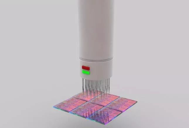
Wafer Testing: At the core level, approximately 10mm/0.5 inches. The image shows a portion of the wafer undergoing its first functional test, using reference circuit patterns for comparison with each chip.
Wafer Slicing: Wafer level, 300mm/12 inches. The wafer is sliced into pieces, each piece being a processor core (Die).
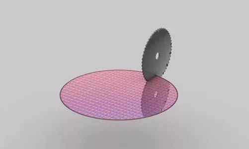
Discarding Defective Cores: Wafer level. Defective cores identified during testing are discarded, leaving intact ones ready for the next step.
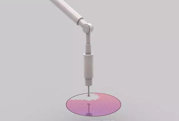
Single Core: Core level. A single core cut from the wafer, here showcasing the Core i7 core.
Packaging: Packaging level, 20mm/1 inch. The substrate, core, and heat sink are stacked together to form the appearance of the processor we see. The substrate (green) serves as a base and provides electrical and mechanical interfaces for the processor core to interact with other parts of the PC system. The heat sink (silver) is responsible for dissipating heat from the core.
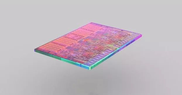
Level Testing: The final test can identify the key characteristics of each processor, such as maximum frequency, power consumption, and heat generation, determining the processor’s grade, whether suitable for the high-end Core i7-975 Extreme or the low-end Core i7-920.

Packing: Processors of the same grade are packed together based on the results of the level testing.

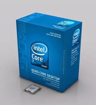
Retail Packaging: The manufactured and tested processors are either delivered in bulk to OEM manufacturers or placed in packaging boxes for the retail market.
– END –
Recommended Excellent Textbook:
Dr. Zhang Yuhong’s “A Simplified Introduction to Artificial Intelligence” book, scan the QR code for detailed information (including supporting teaching outlines, teaching materials, exercise answers, and source code, follow the public account and reply “A Simplified Introduction to Artificial Intelligence” to download relevant materials):

Copyright Statement


Previous Must-Read Articles (Click to View):
1. A comprehensive breakdown! Tracing the origins of ChatGPT’s various capabilities
2. A lengthy article: A detailed explanation of the development history of modern AI and deep learning
3. AI for Science’s first half: How artificial intelligence redefines the new paradigm of scientific research?
4. Why did the Soviet ternary computer get eliminated by binary?
5. Turing Award winner Jack Dongarra: The integration of high-performance computing and AI, how it disrupts scientific computing
6. Turing Award winner Pearl: Looking forward to a mini-revolution that allows machines to understand “why”