
The mantis catches the cicada, while the yellow sparrow is behind
Written by | Wu Hantao
Edited by | Liu Mengdi
1. Background Introduction
With the rapid development of the Internet of Things and electronic devices, fault injection attacks pose an increasing security threat to electronic devices. Fault injection attacks disrupt the normal operation of cryptographic algorithms by inducing internal logical errors in chips (such as voltage fluctuations and clock glitches). Currently, there are many effective protective measures against fault injection attacks, among which a classic measure is the use of fault detection circuits to detect such attacks. When a fault detection circuit detects an attack, the attacked device will either re-execute or not output faulty results, preventing the attacker from exploiting the faulty output.
At the 2024 CHES conference, a research team from the University of Bergen in Norway, KU Leuven in Belgium, and Philips Leuven proposed a method for bypassing fault detection circuits. This method allows for fault injection while remaining undetected by the fault detection circuit, and the research team conducted related experiments on FPGA to verify the effectiveness of the bypassing method.
2. Basic Principles
(1) Timing Violation and Detection Principles
The following diagram shows the structure of a CMOS inverter circuit, where its propagation delay is mainly caused by the charging and discharging delay of the load capacitance. Therefore, when larger gates or multiple gates are combined to form combinational logic circuits, the overall propagation delay will increase.
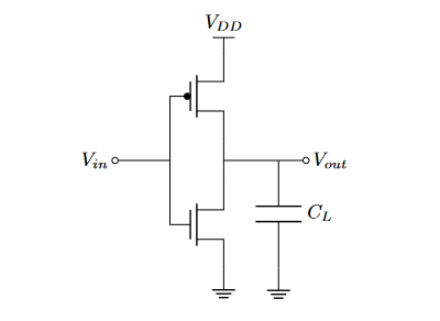
CMOS Inverter Circuit
A common design for fault detection circuits based on timing violation detection is the Parallel Delay Lines (PDL) circuit. The PDL circuit starts with a D-type flip-flop (called the Launch Flop), which toggles its output on each rising edge of the clock, and this output is connected to two different parallel paths with varying propagation delays. The ends of these two paths are connected to an XOR gate, and the output of the XOR gate is sampled by another flip-flop (called the Capture Flop).
When a timing violation fault occurs, the propagation delays of the two parallel paths become very close, causing the XOR gate to produce an abnormal output. If the abnormal output of the XOR gate is sampled by the Capture Flop, it will trigger an alarm in the fault detection circuit. The following diagram shows three common variants of the PDL circuit design, with the main difference being the positions of the XOR gate and the Capture Flop. For the PDL-2 and PDL-3 circuits, the authors assume that the alarm signal from the XOR gate is followed by a D flip-flop for synchronous sampling.
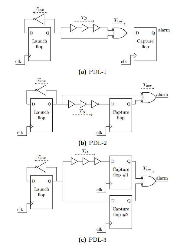
Three Variants of PDL Circuit Design
(2) Bypassable Fault Injection Methods
The authors proposed four fault injection methods that can bypass the protection of the aforementioned three fault detection circuits. Below are the introductions to the four fault injection methods:
Fault Injection Method 1: Launch Flop Failure
Applicable Scenarios: PDL-1 and PDL-2 Fault Detection Circuits
Principle: When the glitch period (TG) is less than the feedback inverter delay of the Launch Flop (Tinv), the Launch Flop cannot complete the state flip, causing the PDL-1 and PDL-2 fault detection circuits to fail to perceive the change. For the PDL-3 fault detection circuit, the authors believe there is a direct connection between the Launch Flop and the second Capture Flop; unless the delay between the two flip-flops is sufficiently large, this fault injection method is not applicable to the PDL-3 fault detection circuit. The following diagram illustrates the principle of Fault Injection Method 1, where clk is the clock signal, and LD and LQ are the data input and output signals of the Launch Flop, respectively.
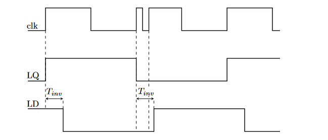
Principle of Fault Injection Method 1
Fault Injection Method 2: Capture Flop Delay Window
Applicable Scenarios: PDL-1 Fault Detection Circuit
Principle: This method utilizes the longer delay of the XOR gate (Txor). After the rising edge of the clock, the first change in the input value of the Capture Flop will occur after Txor. If the glitch period (TG) satisfies the condition Tinv + Tsetup < TG < Txor, then the output LQ of the Launch Flop will change. However, since TG < Txor, the Capture Flop will still sample a low level, so even if this is a clear timing violation, it will not trigger an alarm. The following diagram illustrates the principle of Fault Injection Method 2, where clk is the clock signal, LQ is the data output signal of the Launch Flop, and CD is the input signal of the Capture Flop.
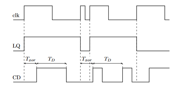
Principle of Fault Injection Method 2
Fault Injection Method 3: Double Glitch Masking
Applicable Scenarios: PDL-2 and PDL-3 Fault Detection Circuits
Principle: Since the alarm signal output from the PDL-2 and PDL-3 circuits requires synchronous sampling, the alarm will only be activated when the output of the XOR gate is high during the rising edge of the clock. The attacker first injects the first glitch. If TG1 < TD (where TD is the delay line propagation path), it will cause the two input values of the XOR gate to differ. By injecting the second glitch before the change propagates through the XOR gate, if the condition TG2 – TG1 < Txor is satisfied, the input values of the XOR gate can be kept equal again. The following diagram illustrates the principle of Fault Injection Method 3, where clk is the clock signal, and the two glitches are the glitch signals, with combined being the clock signal after the glitches are added.
Principle of Fault Injection Method 3
Fault Injection Method 4: Capture Flop Delay Window Extension
Applicable Scenarios: PDL-1 Fault Detection Circuit
Principle: This attack method exploits the vulnerability of the PDL-1 circuit when handling multiple fast glitches. Since there is no direct connection between the Launch Flop and the Capture Flop in PDL-1, the propagation path of the alarm signal has a delay of TD + Txor, causing the detection response to lag behind the glitch event. Thus, the first glitch creates a safe window, allowing the attacker to inject a second fault between TG1 + Txor and TD + Txor without being detected. This method allows the attacker to choose the timing of the second glitch injection over a larger time range, thereby increasing the success rate of the attack. The following diagram illustrates the principle of Fault Injection Method 4.
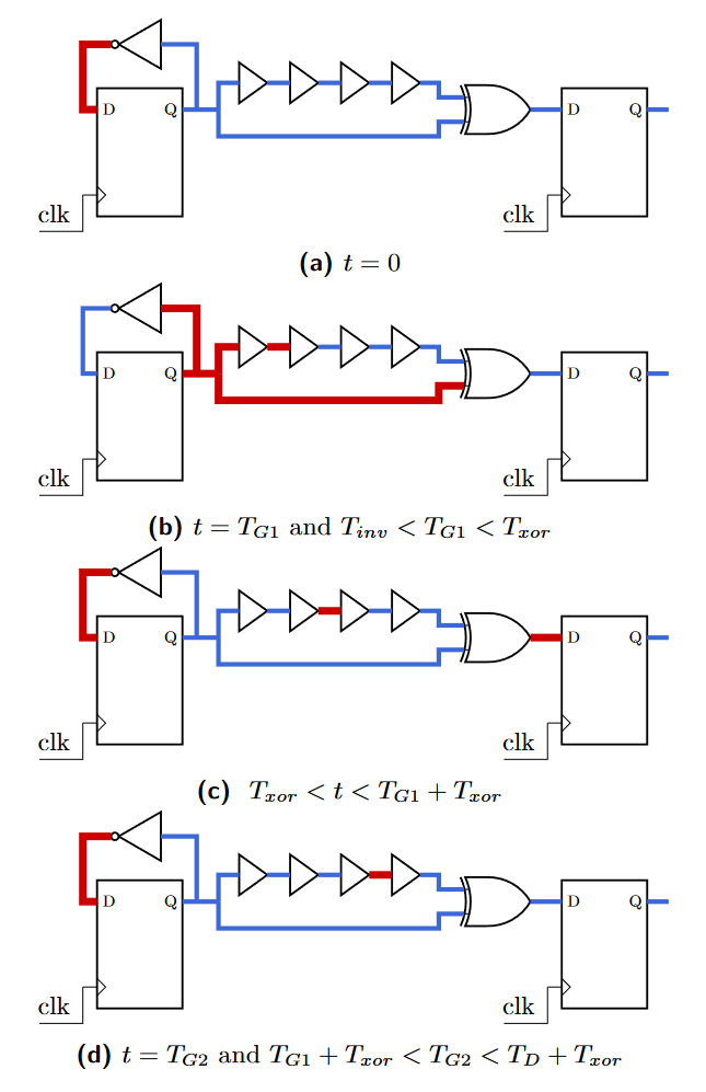
Principle of Fault Injection Method 4
3. Experimental Content
The paper used the CW305-A100 Artix-7 FPGA board from NewAE Technology as the experimental platform. Two parallel AES-128 algorithms and three fault injection detection circuit designs (PDL-1, PDL-2, and PDL-3) were implemented on it. The experiment provided both internal and external clock glitch generators; the internal glitch was generated by the phase-adjustable clock signal from the Xilinx MMCM module on the experimental FPGA board, while the external glitch generator was implemented by an independent FPGA board. The interface of the target device allows for selecting keys and plaintext before each encryption, and after encryption, it can read the generated ciphertext and whether any timing violations were detected.
The experiment first conducted single glitch and double glitch attacks using the internal glitch generator, and repeated the previous experiments with the external glitch generator, studying the impact of voltage on fault injection detection.
(1) Single Glitch Attack
The paper first conducted a single glitch attack experiment, introducing additional glitches into the clock signal during the 9th round of the AES algorithm implementation. The internal glitch generator was used in these experiments. Different periods of clock glitches were injected at the same fault location, with each period being tested 100 times, recording the correctness of the resulting ciphertext and the status of the alarms.
The following diagram shows the stacked histogram of the probability of alarm status after 100 experiments with glitch periods (TG) ranging from 0 to 10 ns.
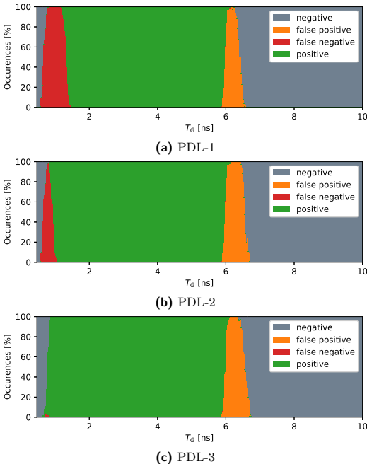
Results of Single Glitch Injection Experiment
It can be seen that when TG > 6.5 ns, the glitch has no effect, and there is a false alarm area between 5.8 ns and 6.5 ns, as the fault detection circuit raises an alarm before the AES algorithm fails. The false alarm rate of PDL-1 is nearly 100% when TG < 1.4 ns. Since Fault Injection Methods 1 and 2 can bypass the detection of PDL-1, the glitch periods for these two injection methods overlap; for PDL-2, only Fault Injection Method 1 can bypass it, so the selectable glitch period range is smaller; PDL-3 has almost no false alarms, indicating that single glitch attacks cannot bypass the protection of the PDL-3 circuit.
(2) Double Glitch Attack
The double glitch attack experiment is similar to the previous single glitch experiment, but two glitches are injected. The specific experimental results are shown in the following diagram:
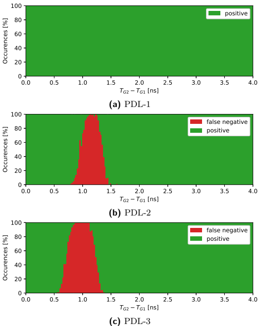
Results of Fault Injection Method 3 (Double Glitch) Injection Experiment
This method can bypass the protections of PDL-2 and PDL-3, and based on the results of the single glitch experiment, the first glitch must trigger an alarm, so the period of the first glitch TG1 is set to 4 ns, and then the values of the second glitch period are traversed. When the interval between the two glitches is less than 1 ns, the false alarm rate of PDL-2/3 approaches 100%.
Finally, the experimental results for Fault Injection Method 4 are shown in the following diagram:
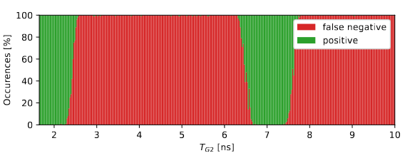
Results of Fault Injection Method 4 (Double Glitch) Injection Experiment
This method can bypass the protections of PDL-2 and PDL-3, and the period of the first glitch must satisfy the conditions of Fault Injection Method 2, i.e., TG1 is approximately 1.1 ns. When the second glitch period TG2 is between 2.5 and 7 ns, satisfying the condition TG1 + Txor < TG2 < TD + Txor, the false alarm rate approaches 100%, which is consistent with theoretical predictions.
(3) External Glitch Generator and Voltage Impact
The paper tested the fault injection performance of the external glitch generator, and the results showed that the external generator could not effectively execute attacks at nominal voltage. The authors then attempted to lower the FPGA core voltage from 1.0V to 0.93V to increase the critical path delay. This also indicates that PDL-type detectors are sensitive to path delay changes, and voltage disturbances can disrupt their calibration thresholds. In actual attacks, a combination of external devices and voltage adjustments can be used to bypass detection under low-cost conditions.
4. Conclusion
The paper reveals the inherent vulnerabilities of PDL-type timing violation detection circuits and proposes four attacks, all successfully verified on FPGA, demonstrating design flaws in existing detection circuits. Current detectors cannot reliably defend against precise timing-coordinated attacks, and defense strategies such as combining PLLs to replace external clock signals and using PDL-1 + PDL-3 in combination are needed.
References
[1] Mosavirik T, Monfared S K, Saadat-Safa M, et al. Silicon Echoes: Non-Invasive Trojan and Tamper Detection using Frequency-Selective Impedance Analysis[J]. IACR Cryptol. ePrint Arch. 2023, 2023:75.
Recommended Previous Articles
-
Laser Command Injection Attacks on Microphone Arrays
-
Hitting the Bullseye: Observing Configuration Bits Inside FPGA Packages with Photon Emission Microscopy
-
A Minimal and Efficient Chip-Level Side-Channel Sensor