Author | Sensor Technology (WW_CGQJS)
Introduction:
With the development of sensors, miniaturization, intelligence, and integration have become essential for upgrades. Today, we will introduce a mini product from the sensor family – MEMS Sensors.
MEMS stands for Micro-ElectroMechanical System. A micro-electromechanical system refers to miniature devices or systems that can be mass-produced, integrating micro-mechanisms, micro-sensors, micro-actuators, as well as signal processing and control circuits, up to interfaces, communications, and power supplies on one or more chips. MEMS sensors are new types of sensors manufactured using micro-electronic and micro-mechanical processing technologies.
MEMS is an advanced manufacturing technology developed based on traditional semiconductor processes and materials. It involves significant interdisciplinary phenomena, mainly involving microfabrication technology, mechanics/solid acoustic theory, thermal flow theory, electronics, materials, physics, chemistry, biology, and medicine. After more than forty years of development, it has become one of the major scientific and technological fields attracting worldwide attention.
MEMS technology is based on mature micro-electronic technology, integrated circuit technology, and their processing techniques. It shares many similarities with traditional IC processes, such as photolithography, thin film deposition, doping, etching, and chemical mechanical polishing processes. However, some complex microstructures cannot be realized using IC processes and must be manufactured using microfabrication technology.
Microfabrication technology includes bulk micromachining, surface micromachining, and special micromachining techniques. Bulk micromachining refers to the etching process along the thickness direction of the silicon substrate, including wet etching and dry etching, which are important methods for achieving three-dimensional structures. Surface micromachining uses thin film deposition, photolithography, and etching processes to deposit structural layer films on sacrificial layer films and then remove the sacrificial layer to release the movable structure.
In addition to the above two microfabrication technologies, MEMS manufacturing also widely employs various special processing methods, including bonding, LIGA, electroplating, soft lithography, micro-molding, micro-stereolithography, and micro-electrodischarge machining.
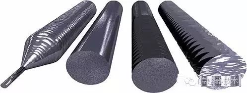
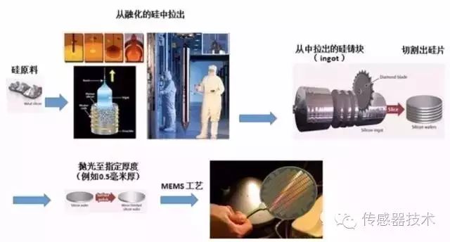
Silicon-based Materials: Most of the raw materials for integrated circuits and MEMS are silicon (Si), a miraculous group VI element that can be extracted in large quantities from silica. What is silica? To put it simply, it is sand. After undergoing a series of complex processing steps, sand becomes single crystal silicon, looking like this:
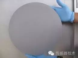
This long pillar, with a diameter ranging from 1 inch (2.5 cm) to 12 inches (30 cm), is cut into layers of 500-micron thick silicon wafers, looking like this:
Using silicon-based materials, the electrical performance is excellent. The strength, hardness, and Young’s modulus of silicon materials are comparable to iron, while its density is similar to aluminum, and its thermal conductivity is close to that of molybdenum and tungsten. If a single MEMS sensor chip has an area of 5 mm x 5 mm, an 8-inch (20 cm diameter) silicon wafer can be cut into about 1000 MEMS sensor chips, significantly reducing the cost per chip.
Non-silicon Materials: In recent years, there has been a trend of non-silicon materials gradually replacing silicon materials in MEMS applications. Academic researchers are now focusing on developing polymer and paper-based micro-devices. Devices made from these materials not only have environmentally friendly processes but also involve simpler equipment and lower costs. Compared to silicon materials, they significantly reduce research and development budgets. Many innovations in polymer and paper-based micro-devices are aimed at medical applications, where biocompatibility and material flexibility are fundamental requirements.
The development of functions and performance for paper-based and polymer micro-devices is still in relatively early stages, and production facilities for such devices have not yet been developed. The maturity and commercialization of these new technologies may take more than ten years. Therefore, there is still much innovative work to be done in silicon-based micro-device research, or it may face the risk of stagnation.
Manufacturing sensors, actuators, or microstructures using MEMS technology features miniaturization, integration, intelligence, low cost, high efficiency, and mass production capabilities, resulting in high production capacity and yield. MEMS technology allows thousands of MEMS chips (some processes also integrate IC chips in the same step) to appear on each wafer, as shown in the following image.
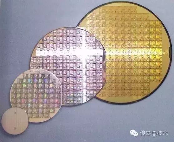
This batch processing has now been fully automated, isolating human factors to ensure that the process errors between each MEMS chip can be strictly controlled, thereby improving yield. After slicing and packaging, they become individual MEMS chips. Visually, most MEMS chips are similar to integrated circuit chips.
In summary, the micron-level feature size allows MEMS sensors to achieve functionalities that traditional mechanical sensors cannot. They are the main force in micro-sensors and are gradually replacing traditional mechanical sensors, widely used in consumer electronics, automotive industry, aerospace, machinery, chemical, and medical fields. Common products include pressure sensors, accelerometers, gyroscopes, electrostatic actuators, DNA amplification microsystems, and catalytic sensors.
Differences from Traditional Sensors:
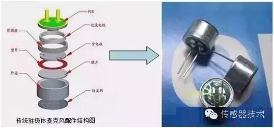
In the image below, we can more clearly understand the differences between traditional microphones and MEMS microphones, taking the microphone as an example.
Traditional Electret Microphone:
MEMS Microphone:
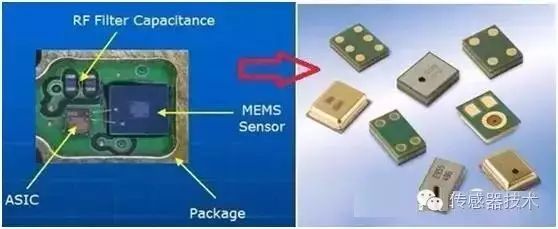
In the image, all the seven or eight mechanical parts of the traditional microphone are integrated into a small MEMS sensor chip, which is very compact and lightweight. Due to chip manufacturing, it has good consistency, low power consumption, and is easier to mass produce. However, the technical requirements are very high. The emergence of MEMS sensors greatly meets the demand for small size and high performance in products.
Classification of MEMS Sensors
MEMS sensors not only can sense the parameters being measured and convert them into measurable signals, but also can analyze, process, recognize, and judge the obtained signals, thus being vividly referred to as intelligent sensors.
MEMS sensors come in various types, and there are many classification methods. Below is a classification based on working principles:
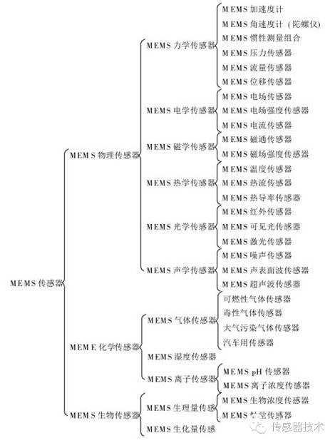
Each type of MEMS sensor has many subdivision methods. For instance, accelerometers can be categorized into angular vibration type and linear vibration type based on the motion of the detected mass. Common MEMS sensors include pressure sensors, accelerometers, micro-mechanical gyroscopes, inertial sensors, MEMS silicon microphones, etc.; the variety of MEMS sensors can reach thousands, and the parameters between different MEMS are quite diverse, with no completely standardized processes.
Let’s watch a video ↓↓↓
As an important strategic industry symbol of international competition, MEMS sensors have attracted global attention due to their high technological content and broad market prospects. In the past decade, China’s MEMS sensor industry ecosystem has gradually improved, forming a complete industrial chain from R&D, design, OEM, packaging, and testing to application, with unprecedented policy support from the state. China’s MEMS industry development faces significant opportunities, especially with the rapid development of mobile internet and the Internet of Things, which will have a profound impact on the MEMS industry and will give rise to numerous new products and applications, driving the popularization of MEMS products in daily life and industrial production.
Editor: Ctrl