Source: Semiconductor Industry Observation (ID: icbank)
Original Author: SRC&SIA
Over the past five years, the sensitivity and accuracy of sensors have improved tenfold, while power consumption, cost, and size have decreased by one-fifth. In the next decade, sensors will need to be more complex, reliable, lower in cost, and equipped with high bandwidth interconnect capabilities to meet the broader applications in wearable devices, artificial intelligence, and autonomous driving.
As the speed of 2D transistor scaling slows and the maturity of 2.5D/3D packaging technologies increases, the development of optical transceivers and interconnect devices using integrated photonics technology, manufactured in CMOS fabs and adopting advanced integrated circuit packaging technologies, is becoming a more significant technological innovation. Optical transceivers co-packaged with data processing (computing) and storage chips are referred to as Co-Packaged Optics (CPO). Chips that contain active photonic devices and associated photonic circuits are called Photonic Integrated Circuits (PIC). These PICs convert electrical signals into optical signals and transmit optical domain data between packages or between the computing core and memory within the package.
The most important value proposition of CPO is increased bandwidth density and energy efficiency, driven by the growing demands for computational power and communication bandwidth. This demand is particularly influenced by the rapid growth and implementation of complex artificial intelligence and ML accelerators and computing clusters, which are pushing the development of interconnect bandwidth, energy efficiency, and lower latency from chip-level systems to large-scale systems composed of thousands of GPUs, CPUs, and memory ICs.
As co-packaged optical transceivers enhance data transmission efficiency, optical sensors and actuators also play an increasingly important role in data collection and processing. These sensors and actuators are critical in products such as televisions, headlights, projectors, and DNA analysis chips, as well as in data sensors and wearable heart rate and oxygen sensors’ optical switches. Many of these sensors are manufactured using Micro-Electro-Mechanical Systems (MEMS) technology. MEMS devices and manufacturing techniques can also be used to adjust, modulate, or regulate the arrangements of optical devices like tunable filters, lasers, and optical fibers, leading to new products such as near-infrared (NIR) material analysis scanners.
Furthermore, the combination of Micro-Electro-Mechanical Systems and Application-Specific Integrated Circuits is also maturing, leading to unprecedented products. The miniaturization of sensors is driving rapid development in areas like telemedicine, smart homes, smart cities, advanced manufacturing facilities, and handheld wearable devices, all of which require sensors that are more complex, reliable, lower in cost, and equipped with high bandwidth interconnect capabilities.
Sensors for the Next Decade
The mobile economy is primarily driven by cost, size, performance, and bandwidth. Strong sensor designs are critical to the success of GPS, gyroscopes, accelerometers, pressure sensors, magnetometers, optical image stabilizers, microphones, and fingerprint sensing in smartphones.In the past five years, the sensitivity and accuracy of sensors have grown tenfold, while power consumption, cost, and size have decreased by one-fifth.These trends are expected to continue.
The integration of physics and artificial intelligence in device computing makes MEMS-based product designs more outstanding. The integration of these sensors enables seamless execution of activities like navigation, stability control, impact detection, adaptive lighting, image stabilization, and traction control. Better sensor performance means higher signal-to-noise ratios (SNR), greater dynamic ranges, and sub-milliwatt power consumption.
There is also a need for sensors with additional functionalities. For example, silicon integrated components with a bandgap smaller than silicon (Si) that can operate in the short-wave infrared (SWIR) range are needed for high-resolution, eye-safe long-range LiDAR. Packaging these sensors in ultra-compact packages is also desirable. Flexible packaging is another emerging area that is very important for wearable devices and medical applications.
Computing and intelligent processing close to the sensor are crucial for energy efficiency and latency, while joint optimization of hardware and software is an important vehicle for collaboration. TinyML (Tiny Machine Learning) is another rapidly developing area in the field of sensors and actuators. This field includes hardware, algorithms, and software on edge devices or near-edge devices. For example, it may be on sensors at the edge of IoT data management and computing solutions. Typically, ML inference on sensor data is done locally, consuming about 1mW.
In the next decade, as TinyML becomes more prevalent and develops in IoT, key areas of focus will include low-power wake-up circuits, non-volatile memory integrated with silicon made using advanced silicon nodes, and ML algorithms that effectively utilize limited memory/computational resources with milliwatt-level power budgets.
Silicon photonic technology is expected to expand frequency and bandwidth for various applications including sensing, interconnects, communication, and computing. Advanced optical sensors for health/medical sensing (including blood glucose monitoring, blood pressure, and heart disease markers) and sensors for automotive applications (such as LiDAR) present significant development opportunities. One key challenge these sensors face is how to achieve the accuracy and reliability of comparable solutions.
To provide true solid-state beam steering for ADAS (Advanced Driver Assistance Systems) LiDAR systems, further development of optical phased arrays and gratings is needed.Solid-state beam steering will reduce costs, improve reliability, and shrink LiDAR scanning systems, all of which are essential for achieving mass production of SAE Level 3 and above autonomous vehicles.
Systems that utilize sensor data often do not perform further safety checks on it, trusting the sensor data instead. Therefore, manipulating the physical phenomena that sensor designs are intended to interpret could lead to undesirable operational processes. For example, a MEMS accelerometer in a smartphone can measure steps simply by playing a YouTube video containing inaudible sounds. Information can even be transmitted using this method.
Thus, the security issues surrounding integrated Micro-Electro-Mechanical Systems (MEMS) devices are a challenge that needs to be addressed to prevent malicious data tampering. MEMS can also be a part of security solutions, as MEMS devices can serve as part of a physical security mechanism to protect circuits from tampering.
Trends in sensor manufacturing and design include:
-
Replacing crystal oscillators with MEMS-based resonators compatible with CMOS to achieve new architectures, higher performance, and eliminate off-chip passive components.
-
Using piezoelectric MEMS sensors and actuators in applications such as handheld ultrasound, as well as improving and miniaturizing speakers and microphones.
-
Employing a full suite of technologies to utilize new low-cost materials and manufacturing techniques to produce lower-cost sensors in high volumes while manufacturing high-precision sensors for critical tasks (such as GPS navigation).
-
Installing sensors in clothing and fabrics to create new fashion categories, competing with sensors based on smartphones, rings, wearables, and watches. Many innovative technologies also have military applications. Fabric sensors pose new demands for connectivity, reliability, and durability.
-
Micro-Electro-Mechanical Systems are driving advances in quantum computing, as MEMS structures are used to achieve communication between qubits and the outside world.
Unlike many electronic products, the manufacturing processes for sensors are diverse and usually tailored to specific applications or types of sensors. Depending on the sensor, it may need to be open to perceive the surrounding environment while also preventing unnecessary environmental influences. Some sensors are better suited for sealed packaging. Key factors in meeting the unique packaging needs of specific sensor structures include the packaging of sensors manufactured using different manufacturing technologies and the integration of flexible and rigid sensors on flexible substrates. One competing trend is that in certain applications, sensor packaging solutions have begun to standardize, thereby improving supply chain efficiency.
There are various ways to integrate sensors with associated electronic devices. Sensors can be built on the same chip through special compatible processes with electronic components, created as post-processing on CMOS above/below, or combined as independent chips. Micro-Electro-Mechanical Systems (MEMS) can also be separated from the CMOS stack, and some researchers even use fin structures as the basis for sensing elements. Separate chips or post-processing can utilize advanced CMOS nodes and optimized MEMS processes. These different integration strategies affect packaging, material selection, manufacturing, and assembly. Each of the aforementioned strategies will have its own advantages in the foreseeable future.
Challenges remain in integrating and achieving power/area efficiency in optoelectronic conversion and interfaces.Addressing these challenges is essential to expand the application scope of this technology.
Future Trends in Communication
Integrated photonic technology will greatly improve communication infrastructure. It is expected that within the next five years, channel symbol rates will easily exceed 100 Gbps, with the aggregate bandwidth of integrated photonic transceiver modules for fiber optic communication reaching 3.2 to 6.4 Tbits/s. The urgent demand for increased bandwidth and energy efficiency will drive the architecture of data centers from pluggable optical devices to co-packaged optical devices (CPO), thereby promoting the transition from copper cables to optical fibers over shorter distances (less than 1 meter).
It must be emphasized that without using Dense Wavelength Division Multiplexing (DWDM) technology (or similar multiplexing methods) to place multiple optical channels on a single fiber, the enormous bandwidth of optical fibers cannot be fully utilized (achieving orders of magnitude increase in bandwidth density through photonic technology). The successful implementation of DWDM or coherent technology on dedicated integrated circuits can also provide trade-offs between channel data rates and the number of channels given a specific fiber bandwidth. This trade-off can improve energy efficiency and reduce system costs. In the coming years, as the bandwidth density of photonic interconnects improves and its applications become more widespread, reducing the energy consumption, per-bit cost, and latency of the entire optical system (especially for AI/mobile computing applications) will become increasingly important.Using short, low-loss channels to package optical devices close to ASICs and other computing integrated circuits will help improve partial energy efficiency and bandwidth, enabling low-power optoelectronic conversion and high-bandwidth data transmission for large-scale systems.
Currently, analog photonic links are used to simplify millimeter-wave node integrated circuit architectures, allowing for over 1000 antennas per chip. Analog photonic links also significantly improve energy efficiency in the process, far exceeding that of digital links in the signal chain.
In communication applications, there is still a vast electromagnetic spectrum that remains undeveloped. To fully exploit this enormous undeveloped spectrum, technological innovation is required. Innovative semiconductor technologies, such as SOI/SiGe-based photonic technologies, VCSELs, micro-LEDs, avalanche photodiodes, and InP-based PICs, will provide advanced process platforms for numerous improvements in future bandwidth and power.
In the field of Micro-Electro-Mechanical Systems, optical switches are replacing OEO switches. MEMS-based tunable filters and capacitors, RF switches, and the aforementioned MEMS resonators are achieving new architectures and higher integration levels, thereby reducing footprint and simplifying packaging. These new components usher in a new era for the design of communication circuits and systems. Utilizing MEMS to achieve tunability, alignment, and calibration of communication elements can also enhance specifications.
Photonics provides significant opportunities to address the power and bandwidth bottlenecks faced by high-performance and data center computing systems in the ongoing data mobility process. New high-speed, low-power transceivers, light sources, waveguides/modulators, and photodetectors are some of the fundamental components of integrated photonics, where sustainable size scalability remains a key challenge. Photonic technology offers opportunities for low-power, high-speed I/O and photonic interconnect structures. Moreover, photonic devices have been shown to perform certain mathematical operations, such as matrix-vector multiplication.
By implementing photonic integration near processors (CPU/GPU/FPGA/ASIC) and in the links from processors to memory, the vast bandwidth and low-loss advantages of optical transmission compared to copper transmission can be leveraged, resulting in bandwidth density improvements of >100 times, energy efficiency improvements of >10 times, and scaling of performance at the package level across the entire system.
Optical links can provide high energy efficiency and low latency interconnects, enabling the decomposition of networks, computing, and memory. This will utilize optical devices co-packaged with ASIC/CPU/GPU and employ optical communication standards to connect computing and memory across racks in hyperscale data centers.
AI accelerators and neuromorphic computing are other exciting areas driving higher compression ratios, with enormous potential for improving energy efficiency when combined with advanced 2.5D/3D packaging integration.
MEMS-based products require more onboard computing to produce smarter sensors. Today, typical MEMS sensors can provide intelligent actions or other processed data. This is part of the smart edge processing trend. The architecture that combines computing and sensing is rapidly changing, impacting CMOS-MEMS integration and advanced packaging.
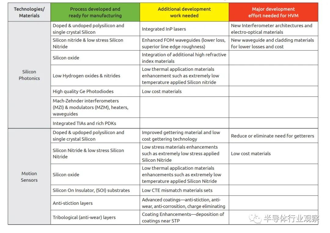
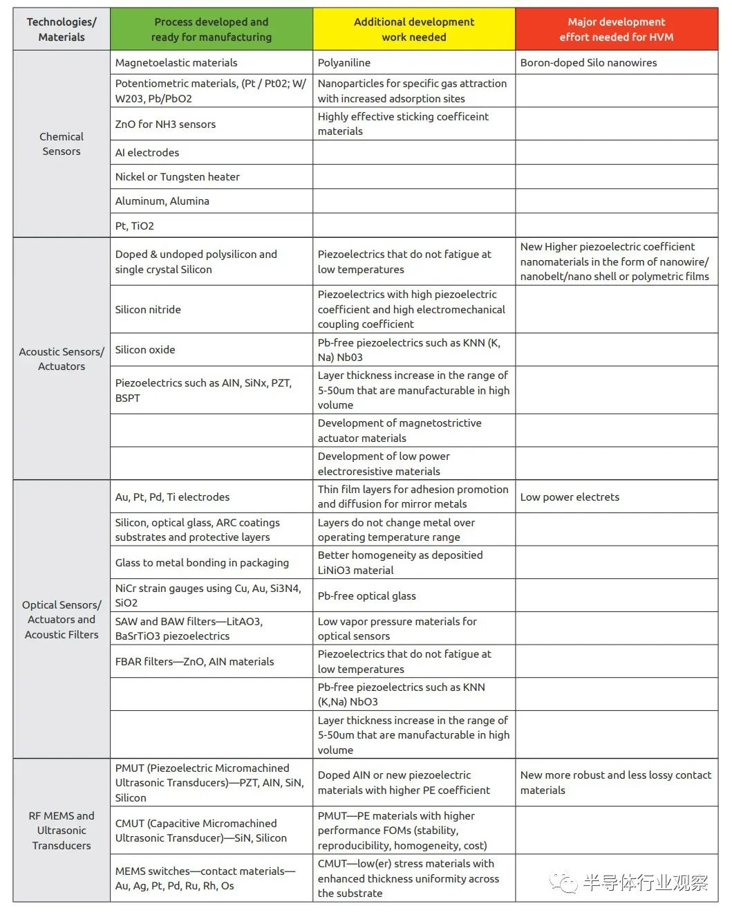
New Materials and Processes
To achieve higher performance and greater integration density, innovative semiconductor process platforms include photonics based on SOI/Ge; integrating III-V materials into silicon wafers through epitaxial growth, wafer/chip bonding, or laser cavity connections for light sources, modulators, and detectors; and active devices based on physical effects beyond plasma dispersion effects (plasma, graphene).
Lithium niobate and barium titanate thin films for hybrid integration are facilitators of high-frequency modulation, while realizing photonic line bonding for laser packaging interconnects using 3D printing technology is another area that requires further research.High bandwidth, low transmission loss, and low-power chip-to-chip optical interconnects are also expected to require advances in embedded waveguides on substrates/PCBs. It is important to ensure low-cost, high-reliability photonic materials that maintain stable performance over extended periods and wide temperature ranges while also maintaining low thermal hysteresis and low-loss characteristics, which requires low overall energy consumption.
For certain sensors and actuators, while improving the performance of inertial sensors and power handling capabilities of RF filters, CMOS-compatible scaling is also needed, necessitating the exploration of new materials such as tungsten or other high atomic mass metals to reduce overall footprint. Additionally, CMOS-compatible platforms based on aluminum nitride are being explored. Furthermore, new piezoelectric and phase-change memory sensors with higher force density and linearity are being studied. These new materials for sensors and actuators will in turn trigger the need for innovations in packaging materials and technologies that require temperature and humidity control.
Two important material drivers for inertial sensors are the ability to prevent mechanical devices from sticking to substrates and a material set with good CTE matching to prevent unnecessary bending and stress, especially bending and stress induced by packaging.These sensors also require improved low-cost acquisition materials and coatings that are wear-resistant, anti-stick, anti-corrosion, and charge-neutralizing. For chemical sensors, the material requirement is to facilitate chemical reactions in a repeatable and stable manner. Some requirements for acoustic sensor/actuator materials (such as microphones/speakers) are to facilitate controlled motion to generate, move, and detect sound.
As these devices must withstand a large number of cycles, a key characteristic of MEMS materials is that their deformation is predictable and does not fatigue. Optical sensor/actuator materials include those that can produce flat, reflective surfaces, are not easily deformed, and possess appropriate optical properties. In RF MEMS switches, developing reliable contact materials remains very important.
In photonics and micro-electromechanical systems applications, several new emerging next-generation materials are worth attention, and the table below lists some examples.
Current Technology Status and Product Examples
Efforts to introduce photonic technology into integrated circuit packaging have already begun. In recent years, some initial products transitioning from standalone transceivers to CPO or optical engines designed for CPO have been showcased.
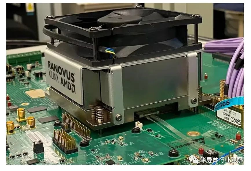
Figure 3 Optical transceiver operating at 896Gbps, integrated with FPGA on the same packaging substrate
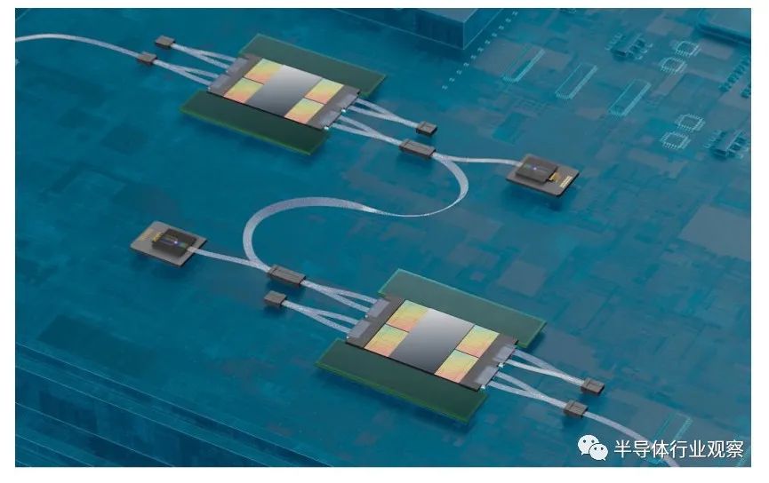
Figure 4 Integration of optical transceivers with data processing integrated circuits
State-of-the-art MEMS products combine multiple sensors with electronic components, providing advanced outputs processed by low-power onboard electronic components, which often integrate artificial intelligence and advanced calibration capabilities. Emerging MEMS products fuse advancements in sensor/actuator manufacturing technologies, materials, and designs. Here are some examples of emerging products:
-
-
Chemical sensors that can sense multiple substances
-
Ultrasound arrays for handheld imaging instruments
-
BAW devices that can be integrated with CMOS
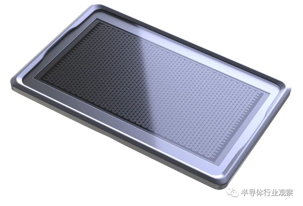
Figure 5 illustrates a state-of-the-art MEMS product—a low-pressure pMUT array chip that combines the proven superior imaging performance of piezoelectric crystals with the cost-effectiveness of silicon. Each chip contains 4096 independently controlled pMUTs, offering large bandwidth, unparalleled sensitivity, and an ultra-wide field of view of up to 150 degrees, enabling rapid improvements in imaging quality and providing real-time AI capabilities to analyze every frame of the image to guide users to find answers immediately. Looking ahead, pMUT technology will enable powerful 3D imaging and has the potential to achieve 4D imaging. Caregivers will be better able to observe patients and make diagnoses faster.
Figure 5 Low-pressure pMUT array chip
Limitations of Existing Technologies
Optical communication is not a new phenomenon. More than half a century ago, with the maturity of fiber optic manufacturing technology and the emergence of III-V technology-based optical emitters and detectors, the role of optical transceivers in long-distance data transmission rapidly expanded, thanks to the low loss, low dispersion, and wide bandwidth characteristics of glass fibers. Advances and diversification in technology have significantly reduced costs, making optical transceivers widely used in access and client applications.
Meanwhile, the emergence of DWDM technology and Erbium-Doped Fiber Amplifiers (EDFA) in the 1990s transformed long-haul networks and laid the foundation for the information superhighway. Over the years, optical transceivers have evolved from custom-designed devices to onboard modules, and then to small form-factor (SFF) pluggable transceivers specified by multi-source protocols. These independent pluggable transceivers play an indispensable role in today’s data centers.
However, with the continuous increase in data volume and computing power of data processing integrated circuits, standalone transceivers are quickly becoming a bottleneck for high-bandwidth data transmission. The total number of transceivers installed on panels may not provide sufficient bandwidth for data processing units or data switches on line cards. As data transmission rates increase to 100 Gigabaud or higher, the copper losses between the serial data switch of the integrated circuit and the optical transceiver data input pins will become a challenge from a signal integrity perspective. Therefore, CPO offers a compelling alternative in this scenario, breaking this physical barrier while continuing to reduce overall system power consumption and costs.
Placing optical transceivers within the same package can address signal integrity issues, as this allows for shorter, lower-loss interconnect devices and potential direct drive optical devices to eliminate long copper wires on line cards.However, to truly overcome bandwidth density bottlenecks, we may need to introduce DWDM technology for long-distance/long-range transceivers while maintaining short-distance co-packaged optical loss mechanisms.
Since MEMS devices often require custom processes, creating a highly standardized platform similar to CMOS is challenging. For example, magnetic sensors may require materials that inertial sensors do not. Some manufacturers are attempting to provide manufacturing processes that produce multiple types of sensors on the same chip, but cost and performance drivers often dictate custom processes. Therefore, the MEMS device manufacturing processes and their related packaging must be designed for coding.
Another limiting factor is the lack of raw components like transistors, as seen in CMOS. Testing methods are often unique to the working principles or applications of sensors, making the testing and assembly infrastructure, ecosystem, and supply chain more complex than for electronic products. Although significant progress has been made in these areas, these issues still limit the widespread adoption of MEMS technology, making time-to-market for MEMS-based products a concern. As the MEMS market continues to grow rapidly, more suppliers will emerge with MEMS products, improving the situation.
Challenges and Possible Solutions
Communication, computing, and memory applications require addressing technical and supply chain challenges across multiple domains:
-
Performance (200G/Lambda +), yield, manufacturability, and cost of photonic ICs (PIC)
-
Low-cost DWDM III-V laser sources for silicon photonics in high-volume production (especially O and C bands)
-
DFB (Distributed Feedback) QDOT and other laser procurement options, performance, electrical efficiency, and cost
-
Non-sealed lasers with high performance at elevated environmental temperatures, suitable for IC packaging environments
-
Integration of high-power lasers with high yield and reliability
-
Hybrid integration of laser materials
-
Passive/active solutions for edge-coupling and vertical coupling fiber connections, scaling and cost of fiber spacing
-
Fiber assembly processes—low coupling loss, high throughput, high yield
-
Optical fiber arrays with high fiber count/density and reduced cladding diameter
-
Development and standardization of interconnect/termination hardware for fiber arrays
-
Fiber management for co-packaged optics (CPO) – high-density fibers (high fiber count) and ribbon fibers per package
-
Advanced heterogeneous packaging, including 3D TSV that achieve high bandwidth density, high SI (signal integrity), and low interconnect power
-
Optical bus architectures for processor-to-processor and processor-to-memory access
-
Low-cost light sources for optical interconnects • Thermal tunability and junction temperature management • Design for testability (DFT) and design for manufacturability (DFM)
-
Stable viable supply chains and ecosystems supporting PICs, lasers, and fiber integration
-
Photonics circuit modeling standards for ecosystem support
Sensor/actuator applications need to address technical and supply chain challenges across multiple domains:
-
Nonlinear reduced-order modeling of sensors/actuators
-
MEMS co-design (sensors/electronic devices and packaging)
-
PDK (Process Design Kit) with material properties across all relevant physical domains
-
Characterization of new materials across all relevant physical domains
-
Material synthesis tools for discovering and optimizing materials with desired properties
-
Characterization of materials under bending and stretching, especially for wearables
-
Standards for material bending and stretching performance
-
FOM standards for sensor performance
-
Reliability and testing standards for emerging technologies
4. CMOS and Multi-Sensor Integration
-
New packaging methods must continue to transition from stacked wire-bonded sensors to achieve greater heterogeneous integration
5. Sensor Design and Manufacturing Improvements
-
Improving inertial sensors to navigation-grade by using field calibration, multiple sensors, and/or combinations with other non-MEMS sensors
-
Improved design and manufacturing methods, as well as enhanced process windows to compensate for manufacturing non-idealities
-
MEMS-based energy harvesters must improve sensor conversion power output percentages to compete with solar and thermoelectric devices
-
Continued development of low-power and near-zero power sensors to meet energy demands
-
Optical glucose sensors must become more accurate to compete with needle-based electrochemical sensors
-
The accuracy of paper and plastic sensors must improve to compete with silicon-based sensors
-
Continue research into atomic clock technologies to replace large components
END
This content is reproduced only represents the author’s views
It does not represent the position of the Semiconductor Institute of the Chinese Academy of Sciences
Editor: March
Responsible Editor: Muxin
Submission Email: [email protected]
1. The Semiconductor Institute has made progress in the research of bionic covering neuron models and learning methods
2. The Semiconductor Institute has made significant progress in inverted structure perovskite solar cells
3. Why is copper used as the interconnect metal in chips?
4. What is the 7nm in chips?
5. Silicon-based integrated optical quantum chip technology
6. How anomalous is the quantum anomalous Hall effect? It may bring about the next revolution in information technology!