
When a PCB board has completed its layout and routing, and there are no errors reported in connectivity and spacing, does that mean the PCB is finished? The answer is certainly no. Many beginners, as well as some experienced engineers, often rush through the process due to time constraints, impatience, or overconfidence, neglecting the post-design inspection. This can lead to basic bugs such as insufficient trace width, component markings overlapping vias, sockets being too close together, and signal loops, among others. These issues can result in electrical or manufacturing problems, and in severe cases, necessitate a complete redesign, leading to waste. Therefore, after completing the layout and routing of a PCB, a crucial step is the post-design inspection.
There are many detailed elements to inspect on a PCB, and I have listed some of the most fundamental and easily overlooked elements for post-design inspection.
1. Component Packaging
(1) Pad spacing. If it is a new component, you need to create the component package yourself to ensure the spacing is appropriate, as pad spacing directly affects the soldering of the component.
(2) Via size (if applicable). For through-hole components, the via size should have sufficient clearance, generally not less than 0.2mm is appropriate.
(3) Silkscreen outline. The silkscreen outline of the component should ideally be slightly larger than the actual size to ensure smooth installation of the component.
2. Layout
(1) ICs should not be placed too close to the edge of the board.
(2) Components of the same module circuit should be placed close together. For example, decoupling capacitors should be near the power pins of the IC, and components forming the same functional circuit should be prioritized in the same area, ensuring clarity in hierarchy and functionality.
(3) Position the sockets according to actual installation arrangements. Sockets are typically wired to other modules, so based on the actual structure, for ease of installation, the proximity principle is generally used to arrange the socket positions, usually close to the board edge.
(4) Pay attention to the orientation of the sockets. Sockets have a specific orientation; if reversed, the wiring will need to be redone. For flat sockets, the socket direction should face outward from the board.
(5) Keep Out areas must not have components.
(6) Interference sources should be kept away from sensitive circuits. High-speed signals, high-speed clocks, or large current switching signals are considered interference sources and should be distanced from sensitive circuits, such as reset circuits and analog circuits. Ground planes can be used to isolate them.
3. Routing
(1) Trace width. The trace width should be selected based on manufacturing processes and current-carrying capacity; the minimum trace width should not be less than the PCB manufacturer’s minimum trace width. Ensure it can carry the required current, generally selecting a width of 1mm/A.
(2) Differential signal lines. For differential lines such as USB and Ethernet, ensure that the traces are of equal length, parallel, and on the same plane, with spacing determined by impedance.
(3) High-speed lines should consider return paths. High-speed lines can easily generate electromagnetic radiation; if the routing path and return path form a large area, it can create a single-turn coil that radiates electromagnetic interference, as shown in Figure 1. Therefore, when routing, ensure there is a return path nearby, and multi-layer boards with power and ground planes can effectively address this issue.
(4) Pay attention to analog signal lines. Analog signal lines should be separated from digital signals, and routing should avoid passing near interference sources (such as clocks and DC-DC power supplies), with shorter routing being preferable.
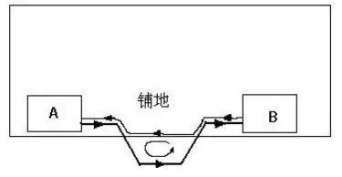
Figure 1
4. EMC and Signal Integrity
(1) Termination resistors. For high-speed or high-frequency digital signal lines that are long, it is best to insert a matching resistor at the end.
(2) Input signal lines should be connected to small capacitors. For signal lines coming from interfaces, it is best to connect a small capacitor close to the interface. The capacitor size depends on the signal strength and frequency and should not be too large, as it may affect signal integrity. For low-speed input signals, such as button inputs, a small capacitor of 330pF can be used, as shown in Figure 2.
(3) Driving capability. For switching signals with larger driving currents, a transistor can be added for driving; for buses with a large fan-out, a buffer (such as 74LS224) can be added for driving.
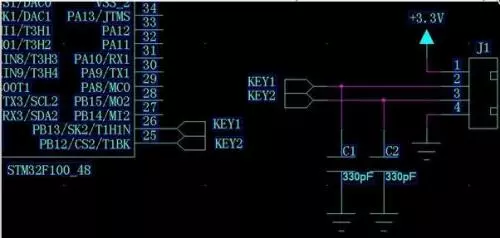
Figure 2
5. Silkscreen
(1) Board name, date, PN code.
(2) Labeling. Label some pins of interfaces (such as arrays) or key signals.
(3) Component markings. Component markings should be placed in appropriate positions, and dense component markings can be grouped. Be careful not to place them over vias.
6. Others
Mark points. For PCBs that require machine soldering, two to three mark points need to be added.


Screenshots from some electronic books

【Complete Set of Hardware Learning Materials】