1. Product Overview
1.1 Application Scope of Junzheng A1 Function Board
The Junzheng A1 is an embedded NVR function board that uses standard DC12V power supply, supports dual SATA hardware interfaces, and is widely applicable to smart NVRs, video decoders, soft routers, and related products.
1.2 Product Overview
The Junzheng A1 features a 1.4GHz dual-core CPU, supporting 4K@90fps decoding, 4K native display, dual Gigabit Ethernet ports, and dual SATA interfaces. In response to the continuously upgrading intelligence requirements of the security industry, the A1 is equipped with 1.4T@int8/5.6@int4 AI computing power, meeting the needs for multi-channel video source synchronization for video structuring, detection, and recognition. Additionally, the A1 integrates key peripherals such as DDR, RTC, and Audio, significantly optimizing product implementation costs.
1.3 Product Features
Onboard dual SATA interfaces, dual Gigabit Ethernet ports, HDMI output, and VGA output. Supports inux+QT system customization, provides system call interface API reference code, perfectly supporting customer upper application APP development and SDK.
2. Product Performance
2.1 Main Chip Block Diagram
2.2 Main Chip Parameters
2.2.1 CPU
XBurst®2 up to 1.2GHz, dual-core, dual-issue, high-performance and low-power implementation of MIPS32 ISA R5
MIPS32 ISA R5 plus Junzheng SIMD512 ISA
Dual-issue, superscalar, superpipelined with simultaneous multithreading (SMT)
— Two hardware threads for each physical core
— Fetch four instructions per cycle
— Dual-issue instructions per thread per cycle
32K L1 D-cache + 32K L1 I-cache, 128~1024K L2 cache
High-performance floating-point unit and SIMD engine: FSE
– Two hardware threads FPU and SIMD units
– Dual-issue FPU and single-issue SIMD units
– 32×512-bit register set per hardware thread, 256-bit load/store to/from SIMD units
– Compliant with IEEE-754 2008 programmable Memory Management Unit (MMU)
– 1st level mini-TLBs (MTLBs)-8×2 entry instruction TLB, 16×2 entry data TLB
– 2nd level TLB: 32×2 entry VTLB, 256×2 entry 4-way set associative XBurst®2 processor system supports little-endian only
2.2.2 MCU
600MHz RISC-V co-processor
32bit, in-order, 5-stage pipeline core
32K L1-cache and 32K L1 D-cache
RV32IM instruction set architecture
2.2.3 AI Engine
Built-in neural network accelerator
Typical performance: 16Tops@int2, 4Tops@int4, 1Tops@int8
Supports int2N-bit (N=1~8) width; shared 1MB memory pool
Magic AI algorithm development platform available
2.2.4 Artificial Intelligence Preprocess (AIP)
Supports multifunctional graphics processing, aip_p (affine/perspective transformation processing), aip_f (scaling processing), aip_t (format conversion processing)
Supports configuration of multiple storage types, data can be accessed from DDR, ORAM
aip_p, aip_f, aip_t can run multithreaded, supports thread protection
2.2.5 Video Decoder & Post Processing
Supports H.264/H.265 video decoder
Supports maximum resolution up to 4K (4096×4096)
Maximum performance: 4096×2160@60fps; supports time-division multiplexing
Pass-through via video decoder to save bandwidth; scaling, cropping
Color conversion, input format: NV12, output formats: RGB888, BGR888, R16G16B16, B16G16R16
Supports dual-channel simultaneous output with different scaling ratios
– First channel supports both reduction and enlargement, input resolution (VGA-2160P), output resolution (VGA-2160P), maximum 3x enlargement
– Second channel only supports reduction, input resolution (VGA-2160P), output resolution (VGA-1080P)
2.2.6 JPEG Codec
Supports encoder and decoder
Supports maximum resolution: 4K (4096×4096)
Encoder maximum performance: 4K@30fps, decoder maximum performance: 4K@30fps
2.2.7 High Definition Multimedia Interface (HDMI)
Video formats:
– All CEA-861-E video formats up to 1080p at 60 Hz and up to 720p/1080i at 120 Hz
– Optional HDMI 1.4b video formats: (depending on configuration)
All CEA-861-E video formats up to 1080p at 120 Hz
HDMI 1.4b 4K x 2K video formats
HDMI 1.4b 3D video mode, up to 340 MHz (TMDS clock)
– Optional HDMI 2.0 video formats: (depending on configuration)
All CEA-861-F video formats
Dynamic Range and Mastering InfoFrame (DRM, packet header 0x87)
Colorimetry:
– 24/30/36/48 bit RGB 4:4:4
– 24/30/36/48 bit YCbCr 4:4:4
– 16/20/24 bit YCbCr 4:2:2
– 24/30/36/48 bit YCbCr 4:2:0
– xvYCC601
– xvYCC709
– Optional HDMI 1.4b colorimetry:
SYCC601, Adobe RGB
Adobe YCC601
Optional color space converter (CSC):
– RGB (4:4:4) to/from YCbCr (4:4:4 or 4:2:2)
Optional HDMI 1.4b supported InfoFrames:
– Audio InfoFrame packet extension to support LFE playback level information
– AVI infoFrame packet extension to support YCC quantization range (Limited Range, Full Range)
– AVI infoFrame packet extension to support content types (graphics, photos, movies, games)
– NTSC VBI infoFrame packet extension to support SCTE 127 payload containing VBI data
Audio formats:
– Uncompressed audio format: IEC60958 L-PCM audio samples
– Compressed audio formats: IEC61937 compressed nonlinear PCM (AC-3, MPEG-1/-2 audio, DTS®)
– MPEG-2/-4 AAC, ATRAC, WMA, MAT)
– HBR audio formats: such as Dolby®True-HD and DTS-HD Master Audio
– Multi-stream audio (L-PCM or IEC61937 compressed nonlinear PCM)
Up to 192 kHz IEC60958 audio sampling rate. Applicable to IEC61937 compressed audio
– HDMI 2.0a: up to 1536 kHz
– HDMI 1.4b: up to 768 kHz
Pixel clock from 13.5 MHz to 600 MHz
Optional removal of pixel duplicate clock from HDMI Tx interface for compatibility with third-party HDMI Tx PHY
Flexible synchronization enable settings for each clock domain functional power-down mode
AMBA APB 3.0 register access
I2C DDC, EDID block read mode
SCDC I2C DDC access
TMDS Scrambler supports 2160p@60Hz with RGB/YCbCr 4:4:4 or YCbCr 4:2:2
YCbCr 4:2:0 support enables 2160p@60Hz at lower HDMI link speeds
Integrated CEC hardware engine
Advanced PHY testability
Synopsys and external PHY interface
Configurable number of rising edge-triggered flip-flops connected for data synchronization
Single-channel DVI 1.0 backward compatibility
2.2.8 Video Display Engine (VDE)
Supports two video layers, GUI layer and mouse layer overlay
Supports HDMI up to 4K@60fps video output, while supporting output formats of RGB, YUV444, YUV422, YUV420
Supports VGA up to 2K@60fps video output, while supporting RGB output format
Supports up to 2K@60fps TFT video output, while supporting RGB output format
Supports simultaneous HDMI and VGA outputs
Supports V0 video layer output enlargement, final output enlargement
V0 video layer supports up to 36 video streams
V1 video layer supports up to 2 video streams
Supported input formats for video layers: NV12/21, NV16/61
Supported input formats for GUI layer: ARGB8888, ARGB1555, compressed images
Supported input formats for mouse layer: ARGB8888, ARGB1555
2.2.9 Image Process Unit (IPU)
Supports single image transfer, filling, flipping, mirroring, clipping, scaling, format conversion
Supports dual-image overlay, color keying, flipping, mirroring, clipping, scaling, format conversion
Supports image compression
Supports input/output formats: NV12, NV21, NV16, NV61, RGB444, RGB555, RGB565, RGB888, ARGB1555, ARGB4444, ARGB8565, ARGB8888
Supports overlay using M1 images
2.2.10 Serial Advanced Technology Attachment (SATA)
SATA 1.5Gb/s, SATA 3Gb/s speeds
Supports two ports; complies with the following specifications:
– Serial ATA 3.3 – AHCI Revision 1.3.1
– AMBA 2.0 and AMBA 3.0 AXI from ARM
Highly configurable PHY interface
User-defined PHY status and control ports
Recovery clock system RX data buffer
Data alignment circuitry
Active LED support
Power management features, including automatic partial sleep transition
BIST loopback mode
Internal DMA engine for each port
Disable RX and TX data clock in power-down mode
2.2.11 Gigabit Ethernet Media Access Controller (GMAC)
Full-duplex RGMII support (1Gbps/100Mbps/10Mbps)
Full-duplex RMII support (100Mbps/10Mbps)
IEEE 802.3az Section 78 (Energy Efficient Ethernet (EEE) features), standard support
1Gbps/100Mbps/10Mbps operation using 4-bit RGMII interface working at 125/25/2.5mHz
System side 64-bit data transfer interface
Little-endian support for sending and receiving data path
Enhanced DMA architecture for better performance and throughput
Supports TCP checksum offloading for received packets (IPv4 and IPv6)
MDIO Master interface (optional) for managing multiple PHY devices and their configurations
Supports TCP segmentation offloading (TSO) feature
2.2.12 Video Output
Video output
– Input format: NV12/NV21 8bit
– Output format: YUV422 8bit
– Output interfaces: 1. BT656 8bit parallel signal; 2. BT1120 8bit parallel signal
– Only supports progressive scan, interlaced scan not supported
– Supports color bar output test
2.2.13 Audio System
Integrated audio codec
– Built-in audio codec
– Single-channel recording, dual-channel playback
– Input supports single-ended or differential, output supports single-ended with echo cancellation
– Supports I2S interface
– Sampling rate supports 8K, 12K, 16K, 24K, 32K, 44.1K, 48K, 96K; AIC/I2S/CODEC
– Supports I2S/MSB-Justified mode serial input and output
– Sampling rate configurable: 8k, 12K, 16k, 24k, 32k, 44.1k, 48k, 96k
– Supports 16, 20, and 24-bit audio sample data sizes; 16-bit packed transmission data is supported
– Supports DMA transfer mode
– Supports interrupt mode to control CPU read/write data
– Supports dual-channel transceiving data, supports half-duplex and full-duplex
– Loopback left channel playback data for echo cancellation
– Supports internal codec and external codec, supports AIC as master/slave external codec
– Supports 6-wire mode and 4-wire mode in external codec
2.2.14 DDR Controller
Typical frequency of 800MHz
DDR PHY can connect one or two KGD
DDR maximum capacity: 4GByte
Memory type: DDR3
2.2.15 Memory Interface
On-chip integrated 2Gbit DDR3
2.2.16 System Functions
Clock generation and power management
– On-chip 2MHZ~30MHZ oscillator circuit, recommended 24MHZ oscillator circuit
– A four-chip phase-locked loop (PLL) with programmable multiplier
– CCLK, HHCLK, H2CLK, H1CLK, PCLK, H0CLK, DDR_CLK frequencies can be changed by setting registers for software
– Functional unit clock gating; timer/counter unit (TCU)
– Includes two TCUs (TCU0, TCU1)
– Includes 0/1/2/3/4/5/6/7 channels (A1 uses channels 0~1)
– General mode: counter counts on clock posedge or negedge or doubling
– Gate mode: counter counts when gate is 0
– Quadrature mode: counter counts due to quadrature input
– Direction mode: counter adds or subtracts due to signal input
– Pos mode: counter starts counting from 0 due to posedge or negedge
– Capture mode: counter counts one cycle and outputs high level time and cycle time
– Internal clock supports 1/4/16/64/256/1024 prescaling
– Can only support exclk and input_clk
– It cannot work in sleep mode
– Does not support exclk 1 prescaling
PWM
– Includes 16 channels, counter clock up to 500MHz. Each channel can be enabled independently
– Two modes for updating PWM configuration: normal update mode and DMA update mode
OS Timer Controller
– 64-bit counter and 32-bit compare register
– Supports generating interrupts when the counter matches the compare register
– Two clock sources: RTCLK (real-time clock), HCLK (system bus clock), selectable 1, 4, 16, 64, 256, and 1024 clock prescaling
– Has counter full match interrupt – counts via external clock (EXCLK), can be 1, 4, 16 prescaled
– Read via synchronous system clock
Interrupt Controller
– Total of 64 interrupt sources
– Each interrupt source can be enabled independently
– Priority mechanism indicating the highest priority interrupt
– All registers are accessible by CPU
– Unmasked interrupts can wake up the chip in sleep mode
Watchdog Timer
– Generates WDT reset
– A 16-bit data register and a 16-bit counter
– WDT has a half-interrupt
– Counter clock uses software-selected input clock
Only RTCLK can serve as the clock for the counter
Clock prescale ratio can be set by software to 1, 4, 16, 64, 256, 1024
Programmable Direct Memory Access Controller
– Supports up to 32 independent DMA channels
– Descriptor or no-descriptor transfer mode compatible with previous positive SoC
– Transfer data unit: 1 byte, 2 bytes, 4 bytes, 16 bytes, 32 bytes, 64 bytes, 128 bytes
– Number of transfer data units: 1 ~ 224 – 1
– Independent source and destination port widths: 8 bits, 16 bits, 32 bits
– Fixed three channel group priorities: 0~3 highest; 4~11 medium; 12~31 lowest
– Bridge from AHB2 to APB
– Data transfer related peripherals: aic, uart0~2, ssi0~1, i2c0~1, des, etc.; OTP from interface
– Total of 2048 bits. And used as 1024 bits to ensure security; Power-On Reset (POR)
– Provides reliable reset functionality for general applications
– Monitors 1.8V power for IO and 0.9V for core
– Typical 1.35V threshold for 1.8V power
– Typical 0.6V threshold for 0.9V power
2.2.17 Peripherals
General I/O ports
– Input/output/function ports configurable
– Low/high, rising/falling edge triggered. Each interrupt source can be masked independently
– Four interrupts, each corresponding to a group, to INTC
– Each port is connected to an internal pull-up and pull-down resistor. Pull-up/pull-down resistors can be disabled
I2C Controller (SMB0, SMB1)
– Two-wire SMB serial interface – consisting of serial data line (SDA) and serial clock (SCL)
– Two speeds: standard mode (100kb/s), fast mode (400kb/s)
– Device clock same as pclk (APB clock) – programmable SCL generator
– Master or slave SMB operation
– 7-bit addressing/10-bit addressing, regardless of configuration as master or slave
– Send broadcast calls or start bytes
– Level send and receive 64 deep FIFO
– Interrupt operation
– The number of devices you can connect to the same SMB bus is limited only by the maximum total bus capacitance of 400pF
– APB interface; SPI Flash Controller (SFC)
– SPI protocol supports Standard, Dual, Quad SPI
– Only send or only receive operations
– MSB first for command and data transfer, LSB first for address transfer
– 64 entries x 32-bit wide data FIFO
– One device select
– Configurable receive sample point
– Configurable timing parameters: tSLCH, tCHSH, and tSHSL
– Supports configurable flash address range
– Transfer formats: standard SPI, dual output/dual input SPI, quad output/quad input SPI, dual I/O SPI, quad I/O SPI, full dual I/O SPI, full quad I/O SPI
– Two data transfer modes: slave mode and DMA mode
– Configurable 6 software process stages
Standard synchronous serial interface (SSI0, SSI1)
– Supports 3 protocols: National’s Micro-wire, TI’s SSP, and Motorola’s SPI
– Full-duplex or only send or only receive operations
– Programmable transfer order: MSB first or LSB first
– 128 entries deep x 32-bit wide sending and receiving data FIFO
– Configurable normal transfer mode or interval transfer mode
– Programmable clock phase and polarity for Motorola SSI format
– Back-to-back character transfer/receive mode
– Loopback mode for testing
– Two slave device select signals, supporting up to 2 slave devices
UART (UART0, UART1, UART2)
– Full-duplex operation
– 5, 6, 7, or 8-bit characters, optional no parity or even parity or odd parity, and 1, 1½, or 2 stop bits
– 64×8-bit sending FIFO and 64×11-bit receiving FIFO
– Independently controlled sending, receiving (data ready or timeout), line status interrupts
– Internal diagnostic capability including loopback control and interrupts, parity, overflow, and framing errors
– Separate DMA requests for sending and receiving data in FIFO mode
– Supports modem flow control via software or hardware
– Slow infrared asynchronous interface compliant with IrDA specification
– Only UART0 supports hardware flow control
MMC/SD/SDIO Controller (MSC0, MSC1)
– Supports SD memory and SD input/output (SDIO) digital interface protocols, compliant with SD HCI specifications
– Supports eMMC Command Queuing Engine (CQE), compatible with CQ HCI specifications
– Supports host version 4
– Supports eMMC specification 5.1
– Supports SD specification 4.1
– Supports SD I/O specification 2.0
– Maximum data rate of 100MBps
– Supports data widths: 1-bit (only dat0 used), 4-bit (dat0 and dat3 used)
– Built-in programmable divider for MMC/SD bus
– Multi-DMA modes: SDMA, ADMA2, ADMA3
– Multi-SD functionality support, including multiple I/Os and combined I/O and memory
– IRQ support enables card interrupts for MMC/SD controller
– Single or multiple block access to the card, including erase operations
– Streaming access for eMMC cards
– Supports SDIO read wait, interrupt detection during 1-bit or 4-bit access
– Supports command completion signal and interrupts to CPU
– Command completion signal disable feature
– Maximum block length of 4KB (4096 bytes)
USB 2.0 OTG Interface
– Port0 supports Battery Charge (BC), OTG (master-slave)
– Port1 supports OTG (master-slave)
– Port2 supports HOST mode only
– Complies with USB 2.0 standard for high-speed (480Mbps) functionality and USB 2.0 On-The-Go supplement
– Supports Session Request Protocol (SRP) and Host Negotiation Protocol (HNP).
– UTMI+ Level 3 transceiver interface
– 16 endpoints
– Supports UTMI+ Level 3 interface (Revision 1.0, February 25, 2004). 16-bit data is supported
– Supports high-speed (HS) mode only
– Supports control, interrupt, ISO, and bulk transfers.
Digital True Random Number Generator (DTRNG)
– Pure digital logic circuit
– True random number
– Interrupt mode and non-interrupt mode
2.2.18 Bootrom
22kB Boot ROM memory
2.3 Board Parameters
Memory: 256MB
Flash: 16MB
Size: 132x70mm
3. Product Peripherals
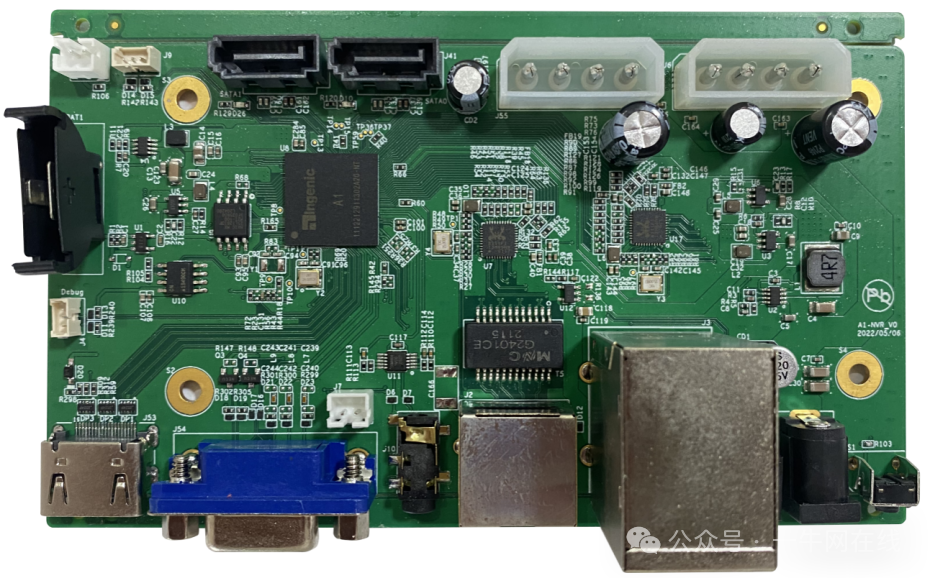
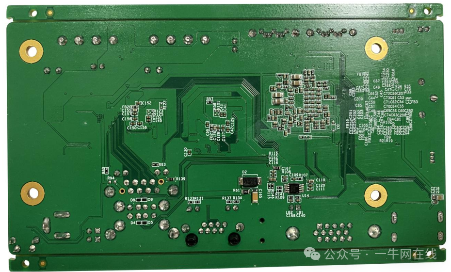
3.1 Appearance Diagram
Front

Back

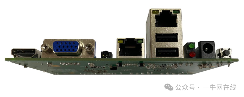
Interfaces

3.2 Board Interfaces
3.2.1 HDMI Interface x1
3.2.2 VGA Interface x1
3.2.3 3.5mm Audio Interface x1
3.2.4 Gigabit RJ45 Interface x2
3.2.5 USB2.0 Interface x2
3.2.6 Power Indicator/Working Indicator x2
3.2.7 DC Power Supply Interface x1
3.2.8 Reset Button x1
3.2.9 SATA Interface x2
3.2.10 D-Type Hard Disk Power Supply Interface x2
3.2.11 TTL Debug Serial Port x1
3.2.12 RTC Battery x1
SigmaStar Low Power Series Chip AI Performance Comparison
SigmaStar Low Power Series Chip AI Performance Comparison (II)
sigmastar& Junzheng & Lianying Solutions
Junzheng T40 NOR Fast AI Camera
Junzheng A1 Full HD Network Video Decoder
Junzheng A1 33-channel (dual network port) streaming device
Junzheng T31ZX+GC4653 4MP PTZ Fixed Focus Camera
sigmastar 120 frames high frame rate smart network camera WIFI module
SC8836Q 2MP HDMI HD Camera Module
SSC8836Q 2MP HDMI HD Camera Module/Customized Solution
sigmastar SSD268G 12MP low-light smart HD network camera module
sigmastar SSC377D 5MP black light full-color smart HD network camera module
RK & Allwinner & Hisilicon Decoding Solutions
RV1103/1106/1109/1126 & RK3562/3568/3576/3588 AI Performance Parameter Selection Guide
Rockchip RK3399 Android Smart Mainboard
Rockchip RK3288 Android 8.1 10.1 inch Dual Screen Smart Interactive Digital Signage
Rockchip RK3288 Wall-mounted WeChat Face Payment Module
Hisilicon Hi3516AV100 Core Board Development Board
Hisilicon Hi3516EV300 Development Board/Core Board
Hisilicon & RK AI Perspective Solutions
Hi3516/3519/3559/3403 AI Performance Parameter Selection Guide
Hisilicon Hi3520 Single SDI Input HDMI Output Encoding Board
Yizhi SV830C Dual Eye (RGB+NIR) Face Recognition
RK3566 Commercial Display Smart Universal Standard Mainboard Solution
Hisilicon Hi3520 Single SDI Input HDMI Output Encoding Board
For more information, please open the link or add the following WeChat, thank you for your attention!
What is Yiniu Network? Let you understand Yiniu Network in 1 minute!

WeChat ID

Long press the QR code to add WeChat
Join the AI technology communication group