With the explosion of emerging industries such as artificial intelligence, 5G communication, and new energy vehicles, the strategic position of semiconductors as an industrial foundation is becoming increasingly prominent.
How is the global semiconductor market size changing? What is the progress of domestic semiconductor industry chain in key areas such as equipment, materials, and components? Can domestic manufacturers achieve breakthroughs in the face of overseas technology restrictions?
Under the support of policies and market demand, what new trends are emerging in various links of the semiconductor industry chain?
This article will comprehensively analyze the current development status, technical difficulties, and domestic path of the three core areas of semiconductor equipment, materials, and components.
The original report has been placed on Knowledge Planet.

This article provides a brief interpretation of the report content.
1. Semiconductor Equipment
1. Market Structure
The global semiconductor equipment market continues to grow. According to SEMI data, the global semiconductor equipment market shipment value in 2023 is $106.3 billion, a year-on-year decrease of 1.3%;
As the cycle low point passes, the market size is expected to reach $113 billion in 2024, a year-on-year increase of 6.4%; by 2025, it is expected to further increase to $121 billion, a year-on-year increase of 7.1%.
Wafer manufacturing equipment is the main component of semiconductor equipment, accounting for about 90%, with thin film deposition equipment, lithography equipment, and etching equipment being the three core devices, collectively accounting for over 60%.
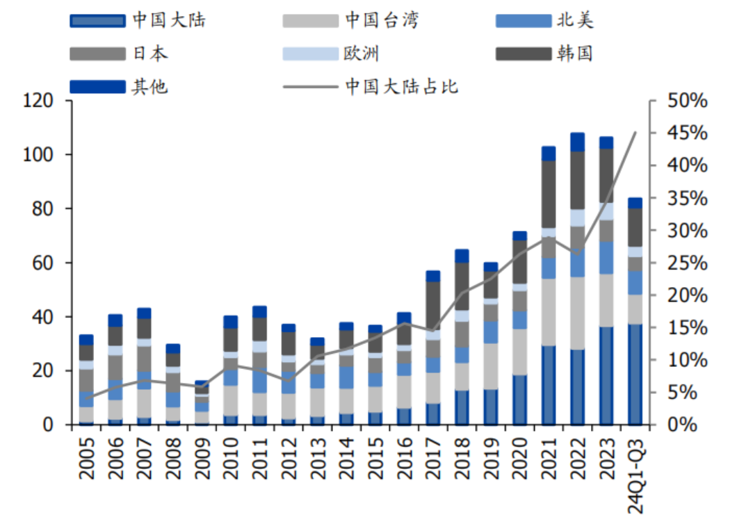
Regionally, mainland China has become the largest market for semiconductor equipment globally.
From 2020 to 2023, the sales share of semiconductor equipment in mainland China has consistently ranked first globally, with a global share of 45% from Q1 to Q3 of 2024, and sales reaching $37.66 billion, leading global market growth.
Taiwan and South Korea follow closely, with expected capacities of 5.8 million wafers/month and 5.4 million wafers/month (8-inch equivalent) in 2025.
Sales of semiconductor equipment by region (in billion USD)
2. Types of Semiconductor Equipment
(1) Lithography Machines
Lithography machines are the core equipment with the highest technical difficulty and cost in chip manufacturing, directly determining the level of chip processing.
Advanced process chip manufacturing requires 60-90 steps of lithography, with lithography costs accounting for about 30% and time consumption accounting for 40-50%.
The core components include lithography light sources, uniform illumination systems, projection lens systems, mechanical and control systems, etc.
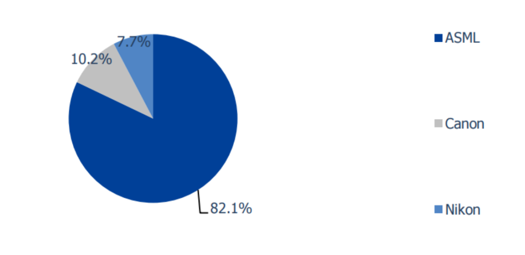
The global lithography machine market is expected to reach $31.5 billion in 2024. The market presents an oligopoly structure, with ASML holding 82.1% market share, while Canon and Nikon account for 10.2% and 7.7%, respectively.
In the ultra-high-end EUV lithography machine field, ASML is the only global supplier; in high-end models such as ArFi and ArF dry, ASML also holds a dominant position.
2022 Global Lithography Machine Industry Competitive Landscape
Domestic lithography machine localization has a long way to go. In 2023, China produced 124 lithography machines, while the demand was 727 machines, resulting in a severe mismatch between supply and demand.
Shanghai Microelectronics is the leading domestic lithography machine manufacturer, having achieved mass production of 90nm process lithography machines and is currently developing 28nm immersion lithography machines.
Due to export restrictions from the US, Japan, and the Netherlands, the import value of lithography machines in China reached $8.754 billion in 2023, a record high, making the localization of lithography machines urgent.
(2) Etching Equipment
Etching equipment transfers mask patterns to the wafer surface through physical or chemical methods and is one of the core devices in semiconductor manufacturing.
According to the process, it can be divided into dry etching and wet etching, with dry etching currently accounting for over 90%, mainly including plasma etching, ion sputtering etching, and reactive ion etching.
Advanced processes drive the growth of etching demand. The production of 7nm integrated circuits requires 140 etching steps, which is 2.5 times more than the 40 steps required for 28nm; the etching steps for 5nm chips reach 160.
3D NAND storage chips have increased the number of stacked layers to 321, requiring etching equipment to achieve a depth-to-width ratio of over 40:1, further driving equipment demand.
The global etching equipment market is dominated by overseas manufacturers, with LAM RESEARCH accounting for 46.7% in 2022, followed by Applied Materials and Tokyo Electron.
Domestic manufacturers are accelerating their catch-up, with North China Innovation’s etching equipment revenue nearing 6 billion yuan in 2023, and Zhongwei Company exceeding 4.7 billion yuan, achieving breakthroughs in dielectric etching, silicon etching, and other fields.
(3) Thin Film Deposition Equipment
Thin film deposition equipment deposits films on the wafer surface through physical or chemical methods, which can be divided into PVD, CVD, and ALD based on the process.
PVD is suitable for the preparation of planar film layers and has a high deposition rate; CVD forms films through chemical reactions and can be applied to insulating layers, metal layers, etc.; ALD has self-limiting growth characteristics, with precise film thickness control, suitable for deep trench structure deposition.
Process upgrades drive an increase in thin film deposition steps. The 90nm CMOS process requires 40 thin film deposition steps, while the FinFET process exceeds 100 steps, with materials increasing from 6 to nearly 20 types.
3D NAND stacked layers have increased to over 400 layers, further increasing thin film deposition steps. The global thin film deposition equipment market is expected to reach $23.96 billion by 2025.
The global market is dominated by Applied Materials, Lam Research, and Tokyo Electron, while domestic manufacturers are gradually breaking through. North China Innovation’s PVD equipment has achieved full coverage of metallization processes for logic and storage chips;
Tuojing Technology’s PECVD equipment has been industrialized in client applications; Zhongwei Company’s CVD tungsten equipment has been validated by storage clients, with significant room for increasing domestic market share.
(4) Measurement and Inspection Equipment
Measurement and inspection equipment includes measurement devices and inspection devices, with the former used to measure film thickness, critical dimensions, and other parameters, while the latter is used to identify defects on the wafer surface, which is a key tool for improving chip yield.
With process upgrades, the requirements for equipment sensitivity, stability, and throughput are higher, and technologies such as optical inspection, electron beam inspection, and X-ray measurement are widely used.
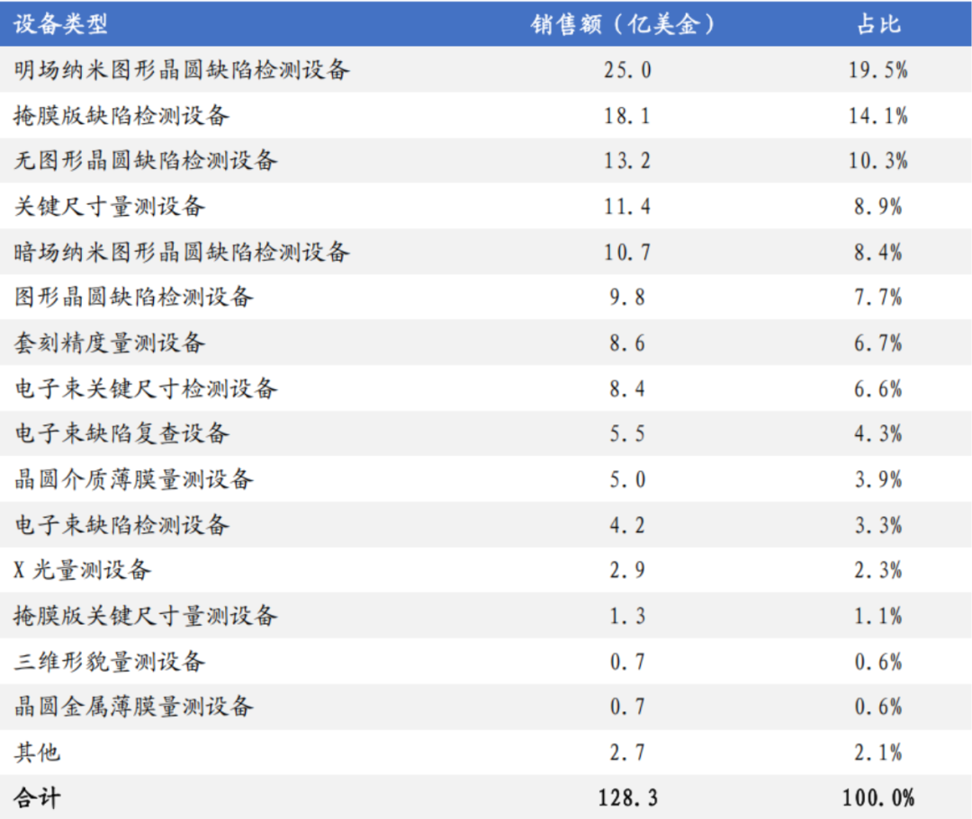
The global semiconductor inspection and measurement equipment market reached $12.83 billion in 2023, with nano-pattern wafer defect detection equipment accounting for 19.5%, making it the largest subfield.
Mainland China accounts for 31.3% of the market, expected to reach $5.19 billion by 2025. The global market is dominated by KLA, while domestic companies such as Zhongke Feicai and Jingce Electronics are accelerating breakthroughs, with bright field/dark field nano-pattern detection equipment already achieving shipments.
Sales and market share of various semiconductor inspection and measurement equipment in 2023
(5) Other Core Equipment
Ion implantation equipment defines the electrical characteristics of chips through precise doping, with the global market expected to reach 27.6 billion yuan in 2024, with AMAT holding 62.65% market share.
Domestic companies such as Kaishitong and Zhongke Xinxin have achieved breakthroughs in low-energy high-current equipment, and North China Innovation is expected to release its first ion implanter in 2025, filling the high-end gap.
Cleaning equipment is used to remove impurities from the wafer surface, with wet cleaning accounting for over 90%.
The global market is dominated by DNS, TEL, and LAM, with DNS accounting for 37% in 2023; domestic Shengmei Shanghai ranks fifth with a 7% market share, with differentiated advantages in acoustic wave and two-fluid technologies.
CMP polishing equipment achieves global flattening of wafers and is used in wafer manufacturing, packaging, and other links. The global market is dominated by Applied Materials and Ebara, accounting for over 90%.
Domestic Huahai Qingke’s CMP equipment market share continues to rise, with the Universal H300 machine receiving bulk orders from leading customers.
3. Localization of Equipment
Domestic equipment manufacturers are experiencing rapid revenue growth. From Q1 to Q3 of 2024, 14 core equipment companies had a total revenue of 45.9 billion yuan, a year-on-year increase of 34%; net profit attributable to the parent company was 8.22 billion yuan, a year-on-year increase of 25.1%.
From 2019 to 2023, the total revenue of these companies increased from 13.81 billion yuan to 50.93 billion yuan, with a CAGR of 38.6%; net profit attributable to the parent company increased from 1.59 billion yuan to 9.59 billion yuan, with a CAGR of 56.7%, and the localization rate increased from 21% in 2021 to 35% in 2023.
Key manufacturers continue to make breakthroughs: North China Innovation, as a platform leader, has achieved large-scale applications in etching and PVD equipment; Zhongwei Company’s etching equipment covers 5nm and more advanced processes; Tuojing Technology’s PECVD equipment shipments are rapidly increasing; Huahai Qingke’s CMP equipment market share is leading domestically; Zhongke Feicai’s measurement and inspection equipment has entered the supply chain of leading wafer manufacturers.
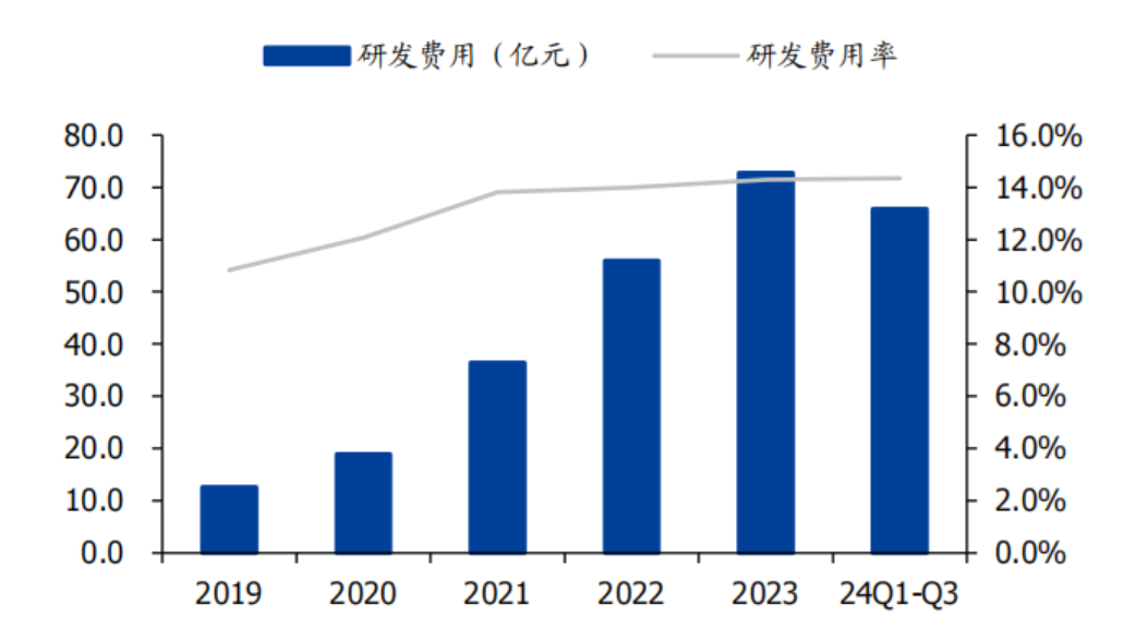
R&D investment continues to increase. In 2019, the 14 equipment companies had a total R&D expenditure of 1.26 billion yuan, which increased to 7.28 billion yuan in 2023, with the expense ratio rising from 10.8% to 14.3%, promoting product category improvement and technology iteration.
R&D expenditure of equipment manufacturers
2. Semiconductor Materials
1. Semiconductor Materials Market
The global semiconductor materials market sales reached $66.7 billion in 2023, a year-on-year decrease of 8.2% due to industry downturn. Among them, wafer manufacturing materials accounted for $41.5 billion, or 62%; packaging materials accounted for $25.2 billion, or 38%.
With AI driving demand growth, the semiconductor manufacturing materials market is expected to grow nearly 8% year-on-year by 2025, with a CAGR of 5.6% from 2023 to 2028, and the scale is expected to exceed $84 billion by 2028.
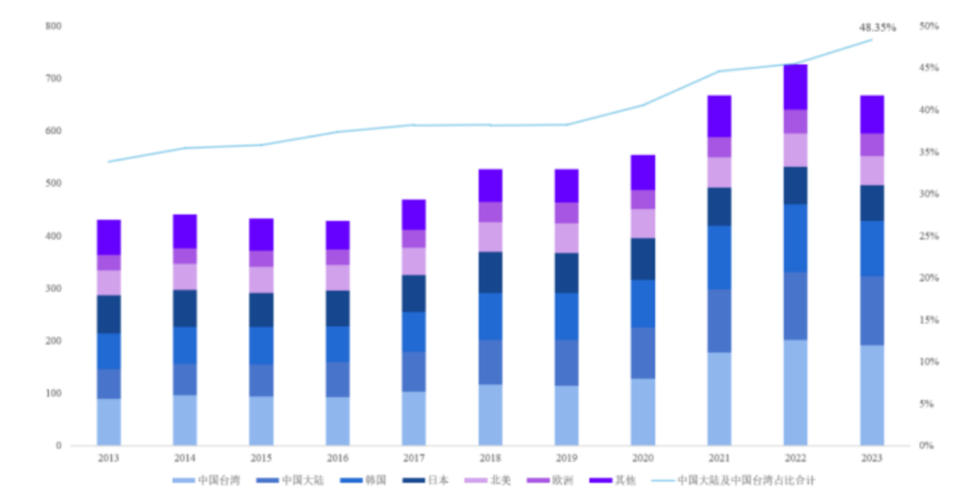
Regionally, Taiwan and mainland China are the top two consumer regions, with sales of $19.2 billion and $13.1 billion in 2023, accounting for 29% and 20%, respectively.
Mainland China is the only region in the world to achieve year-on-year sales growth in 2023, with significant room for domestic substitution.
Global Semiconductor Materials Market Size by Region (in billion USD)
In the semiconductor materials subfield, silicon wafers have the highest share at 33%; gases account for 14%, photoresists and auxiliary materials account for 13%, CMP polishing materials account for 7%, wet electronic chemicals account for 4%, and sputtering targets account for 3%.
The localization rate of high-end materials such as photoresists and electronic gases is less than 30%, making them key areas for domestic substitution.
2. Key Material Types
(1) Silicon Wafers
Silicon wafers are the core substrate material for integrated circuit manufacturing, accounting for 33% of the semiconductor materials market in 2022. They can be classified by size into 12-inch (300mm) and 8-inch (200mm), with 12-inch wafers becoming the market mainstream, accounting for 73.2% of the shipment area in 2023.
Large-size silicon wafers can reduce the unit chip cost, with 300mm wafers having more than double the usable area of 200mm wafers, achieving a usage rate of 2.5 times.
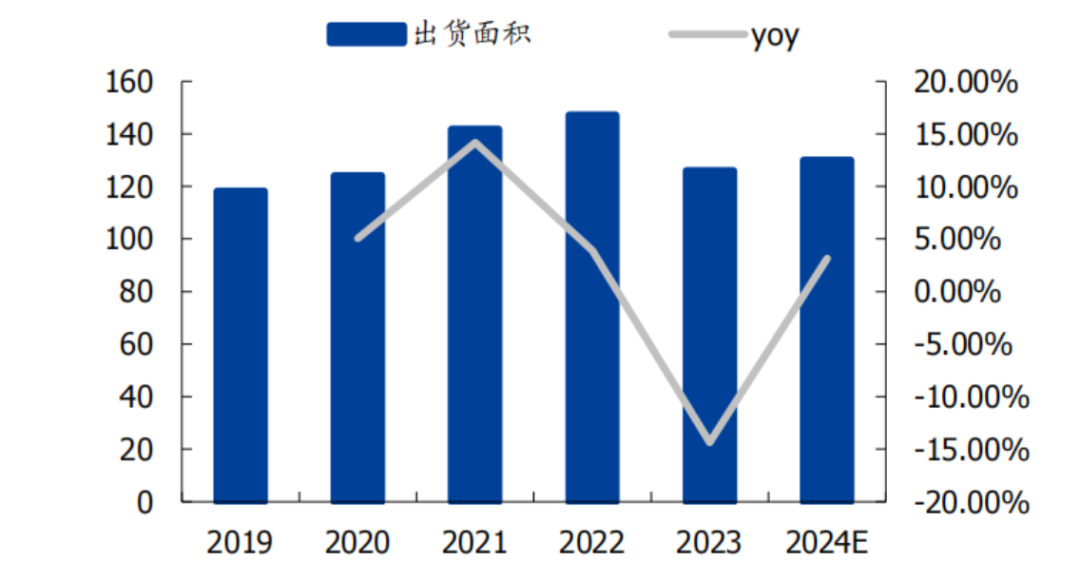
In 2023, the global shipment area of semiconductor silicon wafers reached 12.6 billion square inches, with a market size of $12.1 billion; affected by weak terminal demand, both figures decreased year-on-year by 14.35% and 12.32%, respectively.
A recovery is expected in 2024, with the shipment area expected to reach 13 billion square inches and the market size expected to reach $13 billion. The global market is dominated by the top six manufacturers, including Shin-Etsu Chemical, SUMCO, and GlobalWafers, accounting for 81%.
Domestic companies such as Shanghai Silicon Industry, Zhonghuan Co., and Lian Microelectronics are accelerating breakthroughs. Shanghai Silicon Industry’s monthly production capacity of 300mm silicon wafers is expected to reach 600,000 pieces by the end of 2024, covering logic, storage, CIS, and other fields;
From 2019 to 2023, the revenue CAGR reached 20.91%, continuously expanding production to ensure supply chain security.
Global Semiconductor Silicon Wafer Shipment Area and Growth Rate from 2019 to 2024 (in billion square inches)
(2) Photoresists
Photoresists are core materials in the lithography process, transferring patterns by changing solubility through exposure to light. They can be classified into PCB photoresists, panel photoresists, and semiconductor photoresists based on application.
Semiconductor photoresists have the highest technical requirements, classified by wavelength into G-line, I-line, KrF, ArF, and EUV types, corresponding to different process nodes.
In 2022, ArFi and KrF accounted for the highest shares in the global semiconductor photoresist market at 40% and 33%, respectively; EUV accounted for only 1%, being at the technological forefront.
The market size of China’s semiconductor photoresists has grown from 2.78 billion yuan in 2019 to 6.42 billion yuan in 2023, with a CAGR of 23.3%, and is expected to reach 15.03 billion yuan by 2028.
The high-end photoresist market is dominated by overseas manufacturers such as JSR, Tokyo Ohka, and DuPont, with low localization rates in China: about 30% for g/i line, about 10% for KrF, and about 2% for ArF.
Domestic manufacturers such as Tongcheng New Materials, Jingrui Electronics, and Nanda Optoelectronics are accelerating R&D, with KrF photoresists entering customer verification and volume production, while ArF photoresists are in the verification stage.
(3) Masks
Masks are high-precision tools that carry pattern designs, used to replicate circuit patterns onto wafers or panels, classified by substrate materials into quartz masks, soda masks, etc.
Downstream applications are mainly in semiconductors and flat panel displays, with semiconductors accounting for 60% of the Chinese market in 2022, and LCDs accounting for 23%.
The global semiconductor mask market is expected to reach $6 billion by 2025, with a CAGR of nearly 7% from 2016 to 2025. 63% of wafer manufacturers build their own factories, while independent third-party manufacturers account for 37%, with mature processes above 28nm relying more on third-party procurement.
The flat panel display mask market is expected to reach $1.32 billion by 2030, with technologies such as LTPO increasing layer requirements, driving market growth.
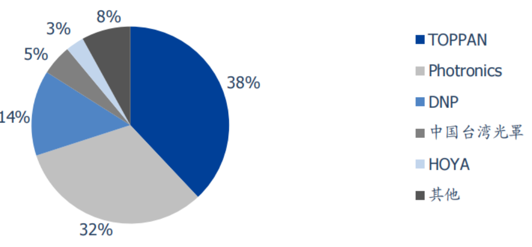
The market is dominated by overseas manufacturers, with TOPPAN, Photronics, and DNP accounting for 84% of the independent third-party semiconductor mask market;
the top four overseas manufacturers in the flat panel display field account for 70%. Domestic companies such as Qingyi Optoelectronics and Luwei Optoelectronics are accelerating breakthroughs, with Qingyi Optoelectronics entering the top five in global market share for flat panel display masks in 2023, and Luwei Optoelectronics advancing semiconductor masks to 130nm-65nm processes.
2023 Global Independent Third-Party Semiconductor Mask Manufacturer Market Structure
(4) Sputtering Targets
Sputtering targets form electronic films through high-energy ion bombardment, consisting of target blanks and backing plates, classified by material into metal targets, alloy targets, and ceramic compound targets.
They are used in semiconductors, flat panel displays, solar cells, and other fields. The semiconductor field has the highest purity requirements, needing to reach above 99.9995% (5N5).
The global sputtering target market size is $25.8 billion in 2023, with a CAGR of 12.52% from 2016 to 2023. The market for semiconductor sputtering targets is $1.95 billion, expected to reach $3.26 billion by 2030, with a CAGR of 6.82%.
The market for semiconductor sputtering targets in China has grown from 1.4 billion yuan in 2017 to 2.3 billion yuan in 2023, with a CAGR of 8.63%, and is expected to reach 3.3 billion yuan by 2026.
Overseas manufacturers occupy 80% of the market share, with JX Metals, Honeywell, and Tohoku Electric being the main suppliers.
Domestic Jiangfeng Electronics has made breakthroughs, ranking second in the global wafer manufacturing sputtering target market in 2022, with products entering the core supply chains of TSMC, SMIC, etc., and achieving a revenue CAGR of 33.3% from 2019 to 2023.
(5) Other Key Materials
Precursors are core materials for film deposition, divided into silicon-based and metal-based precursors, with a global market size of $2.37 billion in 2022, expected to reach $5.44 billion by 2029, with a CAGR of 10.9%.
Merck, Air Liquide, and YAC Technology are the main manufacturers, with the Chinese market expected to reach 17.99 billion yuan by 2028, with YAC Technology’s HCDS, TMA, and other products achieving supply.
Wet electronic chemicals are used in wet cleaning, etching, and other processes, divided into general and functional types. The global market size is $68.402 billion in 2023, expected to reach $82.785 billion by 2025.
The Chinese market is $22.5 billion in 2023, expected to reach $29.275 billion by 2025, with Xingfu Electronics being the domestic leader in electronic-grade phosphoric acid, and Tiancheng Technology accelerating the volume of functional wet chemicals.
Electronic special gases are known as the blood of the electronics industry, used in lithography, etching, and other links. The global market is $5.6 billion in 2023, expected to reach $6.4 billion by 2025;
the Chinese market is 24.9 billion yuan, expected to reach 27.9 billion yuan by 2025. Huate Gas and Jinhong Gas have achieved partial product import substitution, with Huate Gas holding over 60% of the domestic market share for lithography gases.
CMP polishing materials include polishing liquids and polishing pads, with polishing liquids accounting for 49% and polishing pads accounting for 33%. The global market is expected to reach $4.4 billion by 2028, with a CAGR of 5.6%.
Anji Technology holds an 8% global market share for polishing liquids, while Dinglong Co.’s polishing pads are entering stable supply, with increasing localization rates.
3. Localization of Semiconductor Materials
Domestic material manufacturers are accelerating platform-based layouts. The selected 13 core material companies achieved a total revenue CAGR of 18.55% from 2019 to 2023, increasing from 15.85 billion yuan to 31.31 billion yuan;
the net profit attributable to the parent company achieved a CAGR of 17.1%, increasing from 1.6 billion yuan to 3.01 billion yuan. From Q1 to Q3 of 2024, the total revenue reached 27.35 billion yuan, a year-on-year increase of 18.1%, indicating that the share of domestic manufacturers continues to rise.
Key manufacturers’ performance: Dinglong Co.’s CMP polishing pads are expected to achieve revenue of 731 million yuan in 2024, a year-on-year increase of 75%; Anji Technology’s polishing liquids are expected to increase their global market share from 5% to 8%;
Shanghai Silicon Industry’s 300mm silicon wafer production capacity is accelerating expansion; YAC Technology’s precursor products have passed verification from multiple customers; Xingsen Technology’s FCBGA packaging substrates are expected to achieve small-scale production by 2025.
Domestic substitution is extending from mid-to-low-end to high-end, with partial substitution achieved in fields such as silicon wafers, sputtering targets, and CMP polishing liquids, but high-end materials such as photoresists, electronic special gases, and high-end masks still rely on imports, requiring continuous breakthroughs in core technologies in the future.
3. Semiconductor Components
1. Components Market
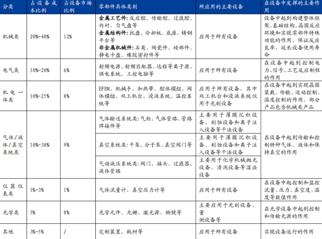
Semiconductor components are the core guarantee of equipment performance, covering mechanical, electrical, mechatronic, gas/liquid/vacuum systems, instruments, and optical components, accounting for 50-55% of equipment costs.
The global market size reached 386.1 billion yuan in 2022, with the Chinese market at 114.1 billion yuan, growing faster than the domestic market, with a CAGR of 15.17% from 2019 to 2023, higher than the global rate of 12.65%.
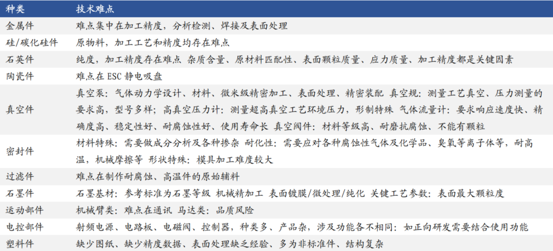
Component technology requirements are stringent, needing to balance precision, strength, cleanliness, and corrosion resistance. The challenges for metal parts lie in processing precision and surface treatment;
the challenges for ceramic parts lie in ESC electrostatic chucks; vacuum parts require no particles and wear resistance; sealing parts need to withstand chemical corrosion and high temperatures, with high difficulty in mold processing.
Challenges in Semiconductor Components
2. Classification of Semiconductor Components
Mechanical components account for 20-40% of equipment costs, including reaction chambers, transport chambers, and gas distribution plates, constructing the overall framework and reaction environment of the equipment to ensure reaction yield.
Electrical components account for 10-20%, such as RF power supplies and power systems, controlling power and process reactions.
Mechatronic components account for 10-25%, including EFEM, robotic arms, and temperature control systems, achieving wafer transport and temperature control, with dual workstations and immersion systems used only in lithography equipment.
Gas/liquid/vacuum systems account for 10-30%, with gas cabinets and vacuum valves used to transport specialty gases and maintain vacuum, mainly applied in dry equipment.
Optical components account for 5%, including optical elements and laser sources, used for light source control and transmission in lithography and measurement equipment. Instrumentation accounts for 1-3%, such as gas flow meters and vacuum pressure gauges, monitoring flow and pressure parameters.
Classification of Semiconductor Equipment Components
3. Localization of Semiconductor Components
The global market concentration is dispersed, with monopolistic structures in subfields, with overseas manufacturers such as ZEISS, Entegris, and MKS Instrument leading.
Domestic manufacturers are accelerating substitution, with 9 core component companies achieving a total revenue increase from 6.77 billion yuan to 18.45 billion yuan from 2019 to 2023, with a CAGR of 28.5%; net profit attributable to the parent company increased from 670 million yuan to 2.56 billion yuan, with a CAGR of 39.7%, growing faster than the domestic market size.
Key manufacturers: Fuchuang Precision achieved a revenue CAGR of 69.0% from 2019 to 2023, with products such as reaction chambers entering the international supply chain; Jiangfeng Electronics is expanding into semiconductor precision components, with applications for both metal and non-metal products;
Zhengtai Technology’s gas delivery system business is growing rapidly, with a year-on-year revenue increase of 45.2% from Q1 to Q3 of 2024.
Domestic manufacturers maintain stable gross margins, with Fuchuang Precision at 25.2%, Jiangfeng Electronics at 29.2%, and Hanzhong Precision at 40.3%. As scale effects become apparent and technology improves, profitability continues to improve.
4. Policies and Markets
1. Policy Support
Multiple policies have been introduced domestically to support the development of the semiconductor industry, including the “14th Five-Year Plan for the Development of the Raw Materials Industry” and “Several Policies for Promoting High-Quality Development of the Integrated Circuit Industry and Software Industry in the New Era,” which clearly promote the localization of equipment, materials, and components, increasing R&D investment and financial support.
Local governments are also taking action, with semiconductor industry clusters in Shanghai, Beijing, Jiangsu, Guangdong, and other regions introducing supporting policies to support enterprises in expanding production, R&D, and talent introduction through tax incentives, subsidies, and industrial funds, building a complete industrial chain ecosystem.
Overseas technology restrictions are forcing domestic substitution. In 2022, the US upgraded semiconductor controls on China, and in 2023, Japan and the Netherlands joined the ranks of export restrictions, limiting the export of advanced equipment and materials, promoting domestic manufacturers to accelerate breakthroughs in core technologies and ensure supply chain security.
2. Market Demand
AI and high-performance computing are driving an explosion in chip demand, with GPUs, AI chips, and others requiring advanced processes and computing power, prompting wafer manufacturers to expand production. By 2025, global wafer capacity is expected to reach 33.7 million wafers/month (8-inch equivalent), with mainland China maintaining double-digit growth, reaching a capacity of 10.1 million wafers/month by 2025.
End markets such as new energy vehicles, 5G communication, and the Internet of Things continue to grow, driving demand for power semiconductors and automotive-grade chips, with significant expansion in mature process capacities, providing application scenarios for domestic equipment and materials.
Advanced packaging technologies are developing rapidly, with 2.5D/3D packaging and HBM technologies enhancing chip performance, driving demand for packaging equipment and materials. The global packaging materials market is expected to exceed $26 billion by 2025, with domestic manufacturers accelerating substitution in packaging substrates, bonding wires, and other fields.
5. Key Enterprises
1. Semiconductor Equipment Enterprises
North China Innovation: A leading domestic semiconductor equipment manufacturer, with products covering etching, PVD, CVD, etc. From Q1 to Q3 of 2024, revenue reached 20.35 billion yuan, a year-on-year increase of 39.5%; from 2019 to 2023, revenue CAGR was 52.7%, and net profit attributable to the parent company had a CAGR of 88.5%. The 12-inch etching machine and PECVD equipment have achieved large-scale applications, with industry-leading technical indicators.
Zhongwei Company: A leader in etching equipment and MOCVD, with expected revenue of 9.065 billion yuan in 2024, a year-on-year increase of 44.7%. The etching equipment covers 5nm and more advanced processes, with high aspect ratio etching machines achieving a production capacity of 60:1; the Preforma Uniflex series of thin film deposition equipment has been validated by clients, expanding the second growth curve.
Tuojing Technology: A leading enterprise in thin film deposition equipment, with PECVD and ALD equipment already in industrial application. From Q1 to Q3 of 2024, revenue reached 2.28 billion yuan, a year-on-year increase of 33.8%. Ultra-high aspect ratio trench filling CVD equipment has achieved shipments, and hybrid bonding equipment is being laid out in the advanced packaging market.
2. Semiconductor Materials Enterprises
Dinglong Co.: A leading domestic CMP polishing pad manufacturer, with expected revenue of 1.56 billion yuan in 2024, a year-on-year increase of 79%. CMP polishing pads have entered stable supply, with polishing liquids and cleaning liquids growing at 180%, and photoresists and advanced packaging materials accelerating verification, building an electronic materials platform.
Jiangfeng Electronics: The second largest supplier of sputtering targets globally, with expected revenue of 3.619 billion yuan in 2024, a year-on-year increase of 39.1%. Products cover advanced and mature processes, entering the supply chains of TSMC and SK Hynix, with a complete layout of semiconductor precision components, expanding growth space.
Anji Technology: A pioneer in polishing liquid domestic substitution, with expected revenue of 1.835 billion yuan in 2024, a year-on-year increase of 48.2%, with a global market share of 8%. Products cover polishing, cleaning, and deposition processes, with the Ningbo base expanding production capacity to meet domestic industry chain demand.
3. Semiconductor Components Enterprises
Fuchuang Precision: A leading manufacturer of precision components, with revenue of 2.31 billion yuan from Q1 to Q3 of 2024, a year-on-year increase of 66.5%. Products such as reaction chambers and transport chambers supply international equipment manufacturers, with a revenue CAGR of 69.0% from 2019 to 2023, showing significant scale effects.
Zhengtai Technology: A provider of gas system solutions, with revenue of 3.5 billion yuan from Q1 to Q3 of 2024, a year-on-year increase of 45.2%. Gas delivery systems and vacuum valves have entered mainstream wafer manufacturers, with breakthroughs in overseas market expansion, including the establishment of a gas production project in Thailand.
6. Future Trends
1. Challenges
High technical barriers: The technology complexity of semiconductor equipment, materials, and components involves precision manufacturing, materials science, optics, and other disciplines, with significant gaps between domestic and overseas in high-end lithography machines, EUV photoresists, and high-purity electronic special gases, requiring long R&D cycles and high investments.
Supply chain risks: Some core raw materials and components rely on imports, with risks of supply disruption due to geopolitical factors, such as high-end optical components and precision vacuum pumps, necessitating the establishment of a self-controllable supply chain system.
Market competition: Overseas giants have leading technologies and well-established layouts, requiring domestic manufacturers to form advantages in cost, service, and technology iteration while coping with industry cycle fluctuations to maintain stable profitability.
2. Trends
Continuous technological iteration: Equipment is developing towards higher precision and higher capacity, with breakthroughs in EUV lithography machines and atomic layer etching technologies; materials are upgrading towards high purity and high performance, with increasing demand for EUV photoresists and advanced packaging materials; components are evolving towards integration and modularization, enhancing equipment performance and reliability.
Increasing localization rates: Driven by policies and markets, domestic equipment is achieving comprehensive substitution in mature processes, with gradual breakthroughs in advanced processes; materials are increasing their shares in silicon wafers, sputtering targets, and CMP consumables, with high-end materials accelerating verification; components are upgrading from single products to modular supply, entering international supply chains.
Combining globalization and localization: Domestic manufacturers are accelerating overseas layouts by establishing production bases and acquiring companies to expand markets; at the same time, deepening local cooperation with wafer manufacturers and equipment manufacturers for joint R&D, forming a collaborative development ecosystem of “equipment-materials-components” to enhance the resilience of the industrial chain.
More new quality industry reports and notes are only published on Knowledge Planet.
Welcome to scan the code to join.

Thank you for your attention, 、
、 