NAND Flash memory is a type of Flash memory that uses a nonlinear macrocell architecture, providing a cost-effective and high-performance solution for solid-state large-capacity memory. NAND Flash memory has advantages such as large capacity and fast rewrite speeds, making it suitable for storing large amounts of data, and thus it has been increasingly widely used in the industry. This article will introduce the working principles and characteristics of NAND Flash.
1. NAND Flash Wafer, PKG, and SSD
NAND Flash Die is cut from a wafer, and a wafer contains many dies. After that, it is packaged into a chip. As shown in Figure 1, a package can contain 1/2/4/8/16 dies, referred to as SDP/DDP/QDP/ODP/HDP respectively. The chip, along with the main controller, DDR, resistors, capacitors, etc., is soldered onto a PCB to form an SSD product.
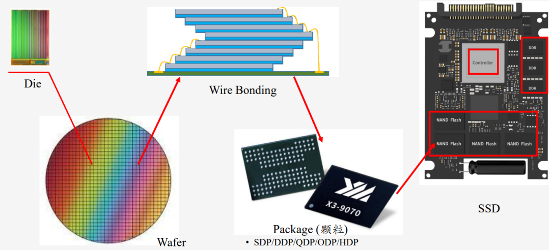
Figure 1
2. History of NAND
Since the world’s first 4MB NAND flash memory was introduced in 1991, subsequent releases included 12MB NAND flash, 1GB NAND flash, and 1GB MLC NAND flash, until 2007 when NAND flash officially transitioned from 2D to 3D technology.
International storage manufacturers have released a roadmap for the next 10 years, indicating that media will continue to evolve. Based on the long-term roadmaps of semiconductor equipment manufacturers and original manufacturers, it is expected that the number of stacked layers in 3D NAND could exceed 500 layers (~2030). In the next three years, it is anticipated that the media storage density (Gb/mm²) will double, and the unit cost ($/GB) will decrease by more than 50%, allowing SSD products built with the latest media to fully enjoy the benefits of technological advancements.
3. Transition from 2D to 3D NAND Flash
The technology of flash memory has evolved from 2D to 3D. The mainstream technology for 2D NAND is Floating Gate (FG), which increases storage density by reducing feature sizes (e.g., from 20nm to 16nm); the mainstream technology for 3D NAND is Charge Trap (CT), which increases storage density by increasing the number of stacked layers (e.g., from 64L to 96L). Currently, the mainstream storage media are based on Charge Trap technology in 3D NAND.
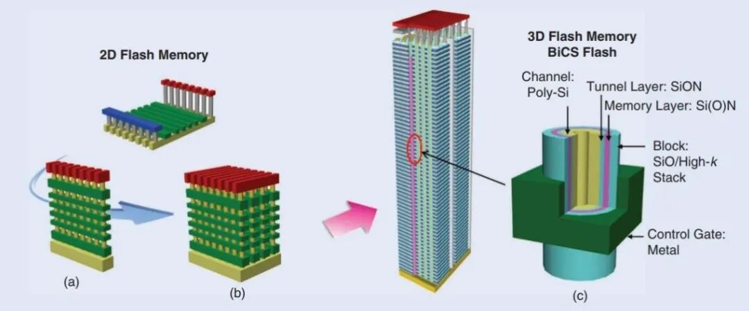
Figure 2
Evolution Trends of 3D NAND
– Multi-Stack
The Multi-Stack technology addresses the challenges of 3D stacking processes, but it introduces additional reliability issues between stacks. Different parameters between layers may exacerbate differences in RBER/tPROG/tR within a single block.
– From CNA to CUA/PUC
The die in flash memory is divided into a storage array and peripheral control circuits, which were originally arranged side by side, known as CMOS Near Array (CNA). As sizes have decreased, the area occupied by peripheral circuits has increased, making cost reduction difficult. Therefore, the storage array has been placed beneath the circuits, known as CMOS Under Array (CUA).
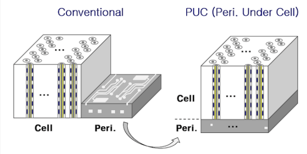
Figure 3
– From TLC to QLC to PLC
As storage density continues to increase, 3D TLC (3 bits/cell) has become the mainstream storage medium, with 3D QLC (4 bits/cell) on the rise. However, as density increases, reliability decreases, so caution is required during application. Currently, PLC (5 bits/cell) is in the experimental technology research phase and will continue to improve storage density.
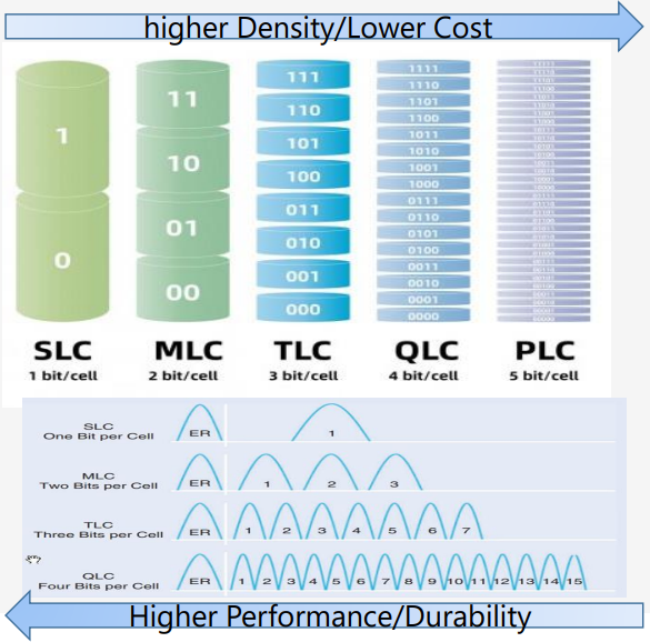
Figure 4
– IOB/Interface Chip
As the speed of media interfaces increases, NAND has introduced interface chips. The current mainstream NAND interface speed is around 2.4Gbps, rapidly evolving towards 3.6/4.8Gbps. When products have requirements for media speed and heavy loads, an IO Buffer (IOB) is needed to enhance the media bus speed.
4. Technical Challenges from Continuous Media Evolution
Media will continue to evolve, bringing challenges in hard disk product design. As the number of layers increases, blocks will become larger. In the future, a block may expand from the current 20-30MB to over 100MB, and if a block is damaged, the contents of over 100MB of capacity will be lost, posing a significant challenge for system management. Additionally, the consistency of read/write latency and error rates, especially the reliability of media at the boundaries formed by multiple stacks in 3D media, requires special attention.
In the next issue, we will continue to share more about the principles and applications of NAND Flash.

Long press to recognize and follow for more Yilian news
Learn more:
History of PCIe® Standard Evolution
What is PCIe?
Yilian SSD End-to-End Data Protection Technology – The “Guardian” of Critical Business