If you need a PDF version of this article without watermark, please send today’s keyword: 230819
This article introduces the integrated workflow for implementing embedded software and FPGA design on the AMD Xilinx Zynq platform, using Simulink for Zynq model design, and methods for integrated hardware/software verification using HDL co-simulation and FPGA-in-Loop. It also discusses the challenges of establishing interfaces between the FPGA and ARM processor, and how to address issues such as design implementation on SoC FPGA, partitioning hardware and software, and generating interface logic. Additionally, the article mentions methods for digital waveform analysis and testing coverage.
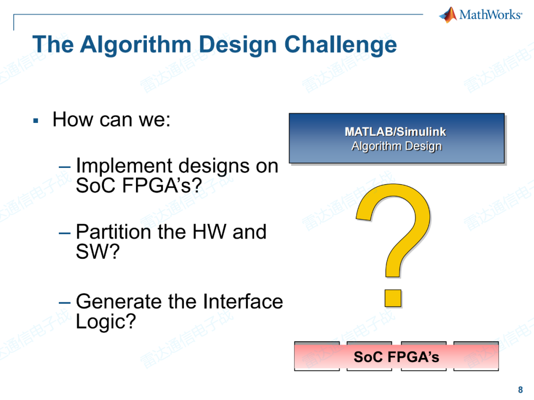
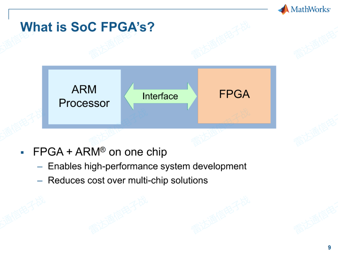
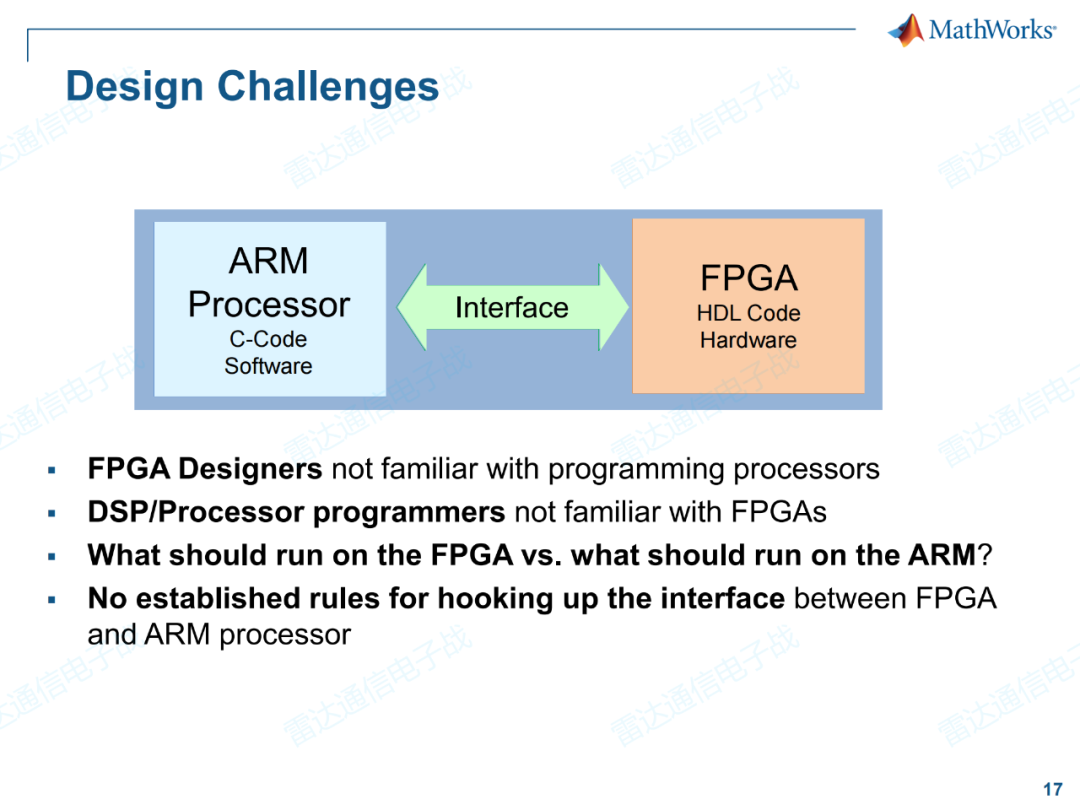
On the Xilinx Zynq platform, the interaction between software and FPGA is achieved through the use of the standard AXI4 interface. This interface allows data transfer and communication between the software and FPGA. In the integrated workflow, it is necessary to first determine which tasks should run on the FPGA and which tasks should run on the ARM processor.
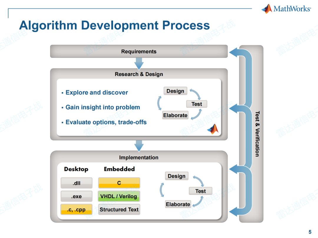
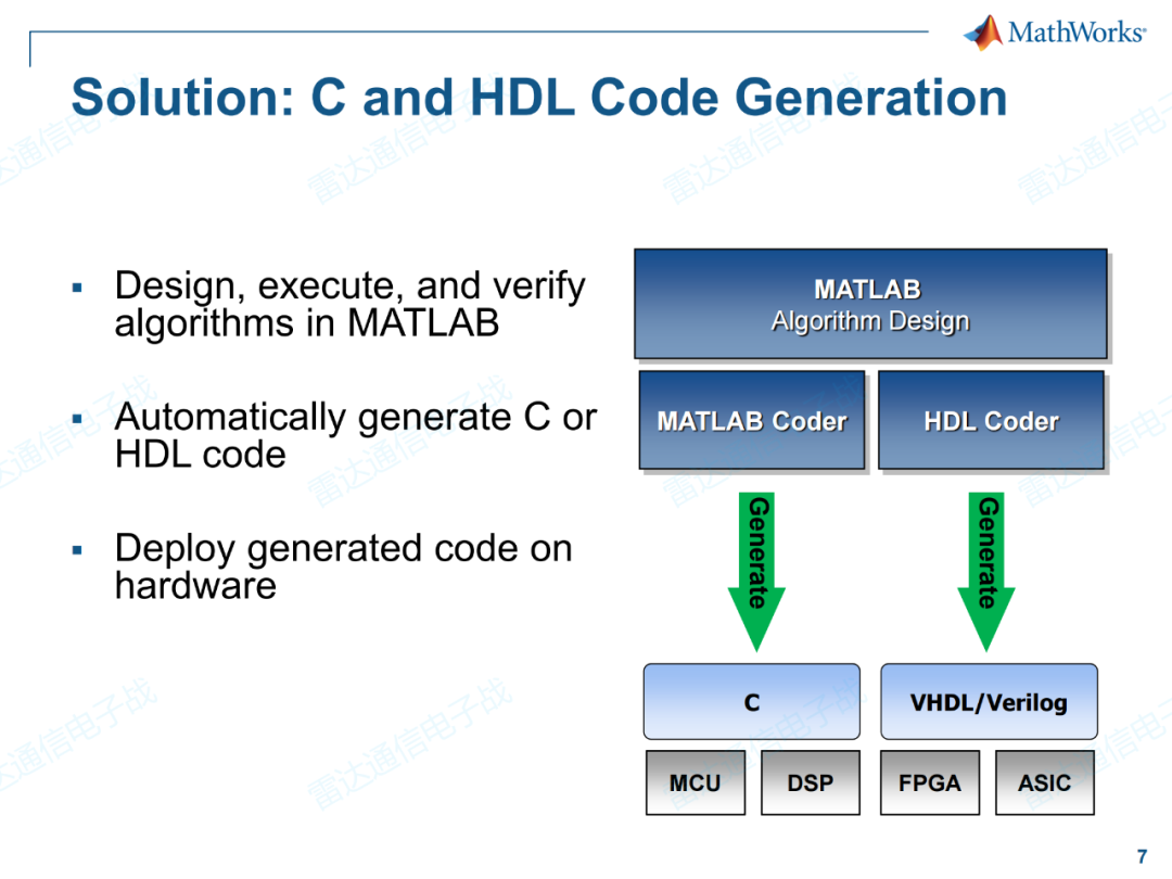
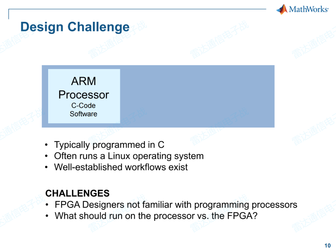
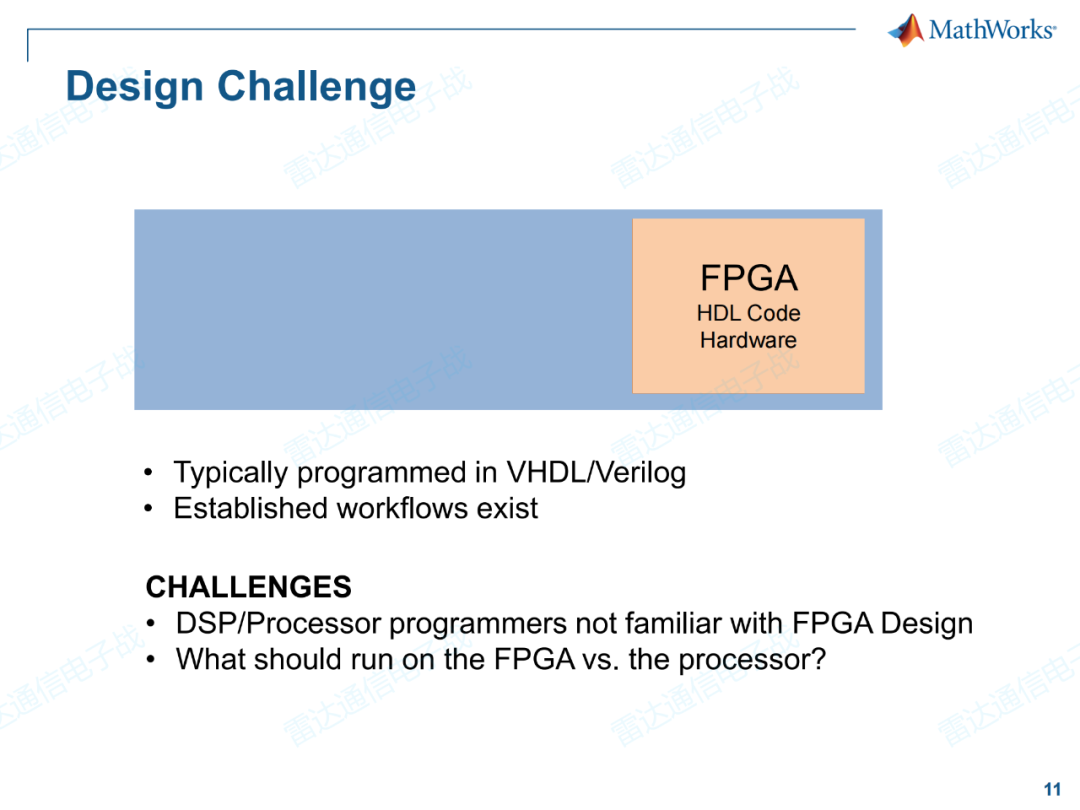
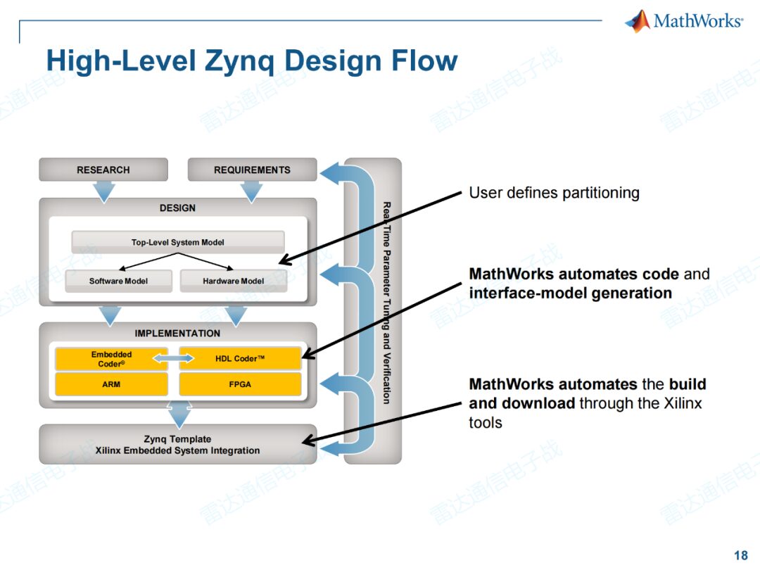
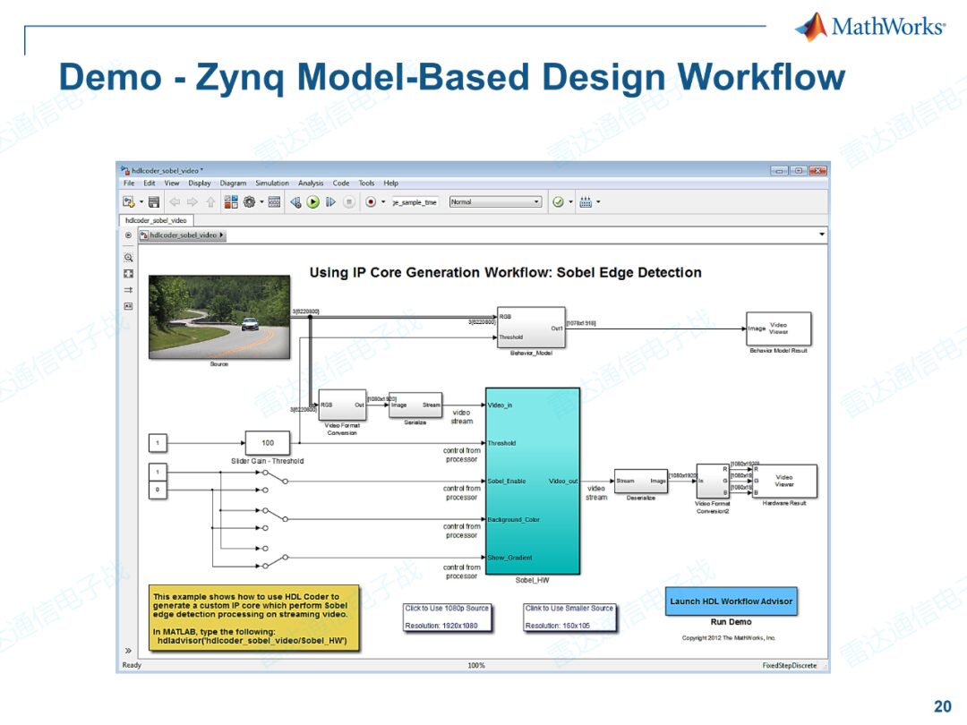
Then, HDL code for the FPGA is written using VHDL/Verilog, and software for the ARM is generated using C code. Next, it is necessary to generate the interface logic and software between the FPGA and ARM. Finally, through integrated HDL verification, the functionality of the entire system is verified using HDL co-simulation and FPGA-in-Loop techniques.When using the Zynq platform for software and FPGA design, the following special considerations and challenges arise:
-
Collaboration Between FPGA Designers and Processor Programmers:FPGA designers are typically not familiar with processor programming, while processor programmers are not familiar with FPGA. Therefore, effective communication and collaboration between the two is essential during the design process to achieve overall system consistency and performance optimization. -
Task Allocation Between FPGA and ARM:During the design process, it is important to clarify which tasks should run on the FPGA and which tasks should run on the ARM processor. This requires a comprehensive consideration of system performance requirements, resource utilization, and power consumption. -
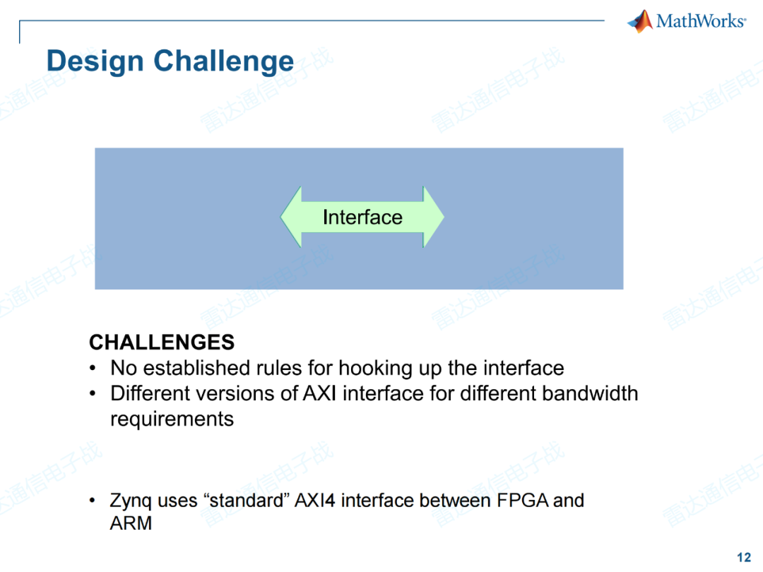
Interface Design Between FPGA and ARM:On the Zynq platform, communication between the FPGA and ARM is done using the standard AXI4 interface. However, correctly connecting and configuring the interface remains a challenge due to the lack of clear rules guiding this process. -
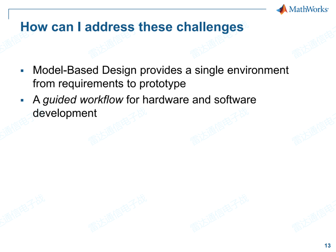
Challenges in Digital Waveform Analysis:During the design process, analyzing digital waveforms can often be quite difficult. Therefore, specific application analysis methods need to be employed to address this issue to ensure the correctness and performance of the design.To tackle these challenges, a Model-Based Design approach can be adopted. By using tools like Simulink, algorithms can be implemented onto FPGA, and the interface logic and software between the FPGA and ARM can be automatically generated. Furthermore, integrated verification methods such as HDL co-simulation and FPGA-in-Loop can be used to validate the correctness of the design. -
System Architecture Design:When using the Zynq platform for software and FPGA design, careful consideration must be given to the system architecture design. This includes determining the communication methods between the FPGA and ARM, the bandwidth and latency requirements for data transfer, and how to partition tasks and collaborate between the processor and FPGA. -
Resource Management and Optimization:The FPGA and ARM on the Zynq platform share resources, such as on-chip memory and clock resources. Therefore, it is necessary to manage and optimize the use of these resources during the design process to maximize system performance and resource utilization. -
System Debugging and Verification:Since software and FPGA designs coexist on the Zynq platform, system debugging and verification become more complex. Appropriate debugging tools and methods, such as hardware debuggers and logic analyzers, are needed to track and analyze system behavior and resolve potential issues. -
Timing and Clock Management:During the design process, careful management of timing and clocks is necessary to ensure the correctness of data transfer and collaboration between the FPGA and ARM. This includes clock domain partitioning, clock handshake protocols, clock division, and clock synchronization. -
Power Consumption Optimization:The FPGA and ARM on the Zynq platform share power, so power consumption optimization must be considered. This includes using low-power design techniques, appropriately configuring power management units, and optimizing algorithms and task allocation. -
Security and Reliability:During the design process, considerations for the security and reliability of the system must be addressed. This includes conducting security analyses and risk assessments, taking appropriate security measures such as encryption, authentication, and protective measures to safeguard the system against malicious attacks and failures. Additionally, reliability analysis and fault-tolerant design are necessary to ensure that the system can continue to operate normally or self-repair in the event of a failure. -
Software Development and Debugging:When developing software on the Zynq platform, appropriate development tools and environments, such as Xilinx SDK and Vivado, need to be selected. Additionally, software debugging and performance optimization must be performed to ensure the correctness and efficiency of the software on the Zynq platform. -
System Integration and Testing:After completing the designs for the FPGA and ARM, system integration and testing are required. This includes integrating the designs of the FPGA and ARM, performing functional verification and performance testing of the overall system to ensure that it operates as intended. -
Version Control and Team Collaboration:In multi-person collaborative projects, version control tools such as Git should be used to manage code versions and changes. Additionally, team collaboration is necessary to ensure that each part of the design can seamlessly connect and work together.
In summary, using the Zynq platform for software and FPGA design is a complex and challenging task. It requires comprehensive consideration of hardware and software design requirements, careful planning of system architecture, optimization of resource utilization and performance, ensuring system security and reliability, and effective debugging and testing. By fully understanding and applying the characteristics and tools of the Zynq platform, efficient and reliable hardware/software co-design can be achieved.