PCB Network City News
Today, we share an article about the IC chip production process. We hope it will be helpful to industry colleagues.
The complex and intricate chip design process
The chip manufacturing process is like building a house with LEGO; it starts with a wafer as the foundation, and then layers of the chip manufacturing process are built up to produce the necessary IC chips (which will be introduced later). However, without a design blueprint, no matter how strong the manufacturing capabilities are, it is useless. Therefore, the role of the architect is crucial. But who exactly is the architect in IC design? This article will introduce IC design next.
In the IC production process, ICs are often planned and designed by specialized IC design companies. Well-known companies like MediaTek, Qualcomm, and Intel design their own IC chips, providing different specifications and performance chips for downstream manufacturers to choose from. Since ICs are designed by various companies, IC design heavily relies on the skills of engineers, and the quality of engineers affects the value of a company. However, what steps do engineers take when designing an IC chip? The design process can be simply divided as follows.
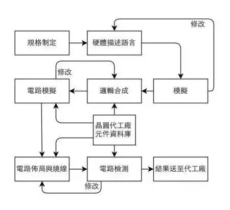
The first step in design is to set goals.
In IC design, the most important step is specification formulation. This step is like deciding how many rooms and bathrooms to have before designing a building and what building regulations need to be followed. After confirming all functions, design can begin, thus avoiding extra time spent on subsequent modifications. IC design also requires similar steps to ensure that the designed chip will not have any errors.
The first step in specification formulation is to determine the purpose and performance of the IC, setting the general direction. Next, we look at which agreements need to be complied with; for instance, a wireless card chip must comply with IEEE 802.11 standards, otherwise, the chip will not be compatible with products on the market, making it unable to connect with other devices. Finally, we establish the implementation method of this IC, allocating different functions into different units and establishing methods for connections between different units, thus completing the specification formulation.
After completing the specifications, the next step is to design the details of the chip. This step is like making preliminary notes of the building plan, outlining the overall shape for easier subsequent drafting. In IC chips, this involves using Hardware Description Language (HDL) to describe the circuits. Commonly used HDLs include Verilog and VHDL, which can easily express the functions of an IC through code. Next, the correctness of the program functions is checked and continuously modified until it meets the expected functionality.
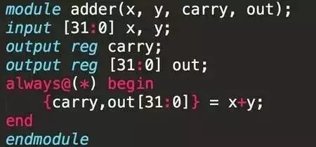 ▲ Example of a 32-bit adder in Verilog
With computers, things become easier.
With a complete plan, the next step is to draw the flat design blueprint. In IC design, the logic synthesis step involves inputting the confirmed HDL code into Electronic Design Automation (EDA) tools, allowing the computer to convert the HDL code into logic circuits, resulting in the following circuit diagram. Afterward, we repeatedly confirm whether this logic gate design diagram meets the specifications and modify it until the functionality is correct.
 ▲ Result after synthesizing the control unit
Finally, the synthesized program code is input into another set of EDA tools for circuit layout and routing (Place And Route). After continuous testing, the following circuit diagram will be formed. In the diagram, different colors such as blue, red, green, and yellow represent different masks. As for how the masks are used,
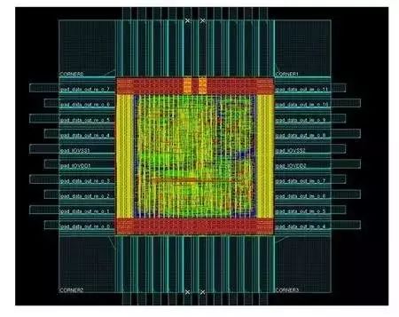 ▲ Commonly used calculation chip – FFT chip, completed circuit layout and routing result
Layer upon layer of masks create a chip.
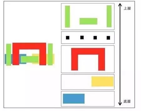
First, it is already known that an IC will produce multiple masks, which have upper and lower layers, each with its own tasks. The following diagram is a simple example of masks, taking the most basic component in integrated circuits, CMOS, as an example. CMOS stands for Complementary Metal-Oxide-Semiconductor, which combines NMOS and PMOS to form CMOS. As for what a Metal-Oxide-Semiconductor (MOS) is? This component widely used in chips is relatively difficult to explain, and general readers may find it hard to understand, so we won’t delve into it here.
In the diagram below, the left side shows the circuit diagram formed after layout and routing, and it has been established that each color represents a mask. The right side shows how each mask is unfolded. The production starts from the bottom layer, following the methods described in the previous IC chip manufacturing, layer by layer, until the desired chip is produced.
By now, there should be a preliminary understanding of IC design. Overall, it is clear that IC design is a highly complex profession, and thanks to the maturity of computer-aided software, IC design can be accelerated. IC design companies heavily rely on the intelligence of engineers; every step described here has its specialized knowledge, which can form multiple specialized courses, such as writing hardware description languages, which requires not only familiarity with programming languages but also understanding how logic circuits operate and how to convert required algorithms into programs, and how synthesis software converts programs into logic gates.
What is a wafer?
In semiconductor news, wafers are often referred to by size, such as 8-inch or 12-inch wafers. However, what exactly is a wafer? What does the 8-inch refer to? What difficulties are there in producing large-size wafers? Below, we will gradually introduce the most important foundation of semiconductors – what a “wafer” really is.
A wafer is the foundation for manufacturing various computer chips. The chip manufacturing process can be compared to building a house with LEGO bricks, stacking layer upon layer to complete the desired shape (which represents various chips). However, without a good foundation, the house will be crooked and not as expected. To create a perfect house, a stable substrate is needed. In chip manufacturing, this substrate is the wafer that will be described next.
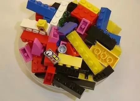 Source: Flickr/Jonathan Stewart CC BY 2.0
First, think back to when you were a child playing with LEGO bricks; the surface of the bricks has small round protrusions that allow two bricks to be securely stacked together without glue. Chip manufacturing also uses a similar method to secure the atoms added later to the substrate. Therefore, a substrate with a smooth surface is needed to meet the conditions required for subsequent manufacturing.
In solid materials, there is a special crystal structure – monocrystalline. It has the characteristic of atoms being tightly arranged one after another, forming a flat atomic surface. Therefore, using monocrystalline to make wafers can meet the above requirements. However, how to produce such materials involves two main steps: purification and crystal pulling, after which such materials can be completed.
How to manufacture monocrystalline wafers
Purification is divided into two stages. The first step is metallurgical-grade purification, which mainly involves adding carbon to convert silicon dioxide into silicon with a purity of over 98% through oxidation-reduction. Most metal refining, such as iron or copper, is done this way to achieve sufficient metal purity. However, 98% purity is still not enough for chip manufacturing, and further enhancement is needed. Therefore, further purification is done using the Siemens process, which yields high-purity polycrystalline silicon required for semiconductor processes.
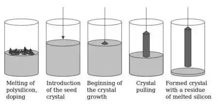 ▲ Silicon rod manufacturing process (Source: Wikipedia)
Next is the crystal pulling step. First, the high-purity polycrystalline silicon obtained earlier is melted to form liquid silicon. Then, a seed of monocrystalline silicon is brought into contact with the liquid surface, and while rotating, it is slowly pulled upwards. The reason for needing a monocrystalline seed is that silicon atoms need a leader to know how to arrange themselves correctly, just like people in a queue; the seed acts as the important leader, guiding the following atoms on how to line up. Finally, after the silicon atoms solidify upon leaving the liquid surface, a neatly arranged monocrystalline silicon rod is completed.
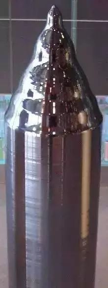
▲ Monocrystalline silicon rod (Source: Wikipedia)
However, what do 8-inch and 12-inch represent? They refer to the diameter of the silicon rod after it has been processed and cut into thin circular slices. What difficulties are there in manufacturing large-size wafers? As mentioned earlier, the process of making silicon rods is like making cotton candy, rotating while forming. Those who have made cotton candy know that making large and solid cotton candy is quite difficult, and the crystal pulling process is similar; the speed and temperature control during pulling affect the quality of the silicon rod. Therefore, the larger the size, the higher the requirements for speed and temperature during pulling, making it more challenging to produce high-quality 12-inch wafers compared to 8-inch wafers.
However, a whole silicon rod cannot be used as a substrate for chip manufacturing. To produce individual silicon wafers, the silicon rod needs to be cut into circular slices using a diamond saw, and the slices are then polished to form the silicon wafers needed for chip manufacturing. After so many steps, the manufacturing of chip substrates is successfully completed, and the next step is the stacking process, which is the chip manufacturing. As for how to manufacture chips,
Layer upon layer of stacking to create chips.
After introducing what silicon wafers are, we also know that manufacturing IC chips is like building a house with LEGO bricks, stacking layer upon layer to create the desired shape. However, building a house involves many steps, and so does IC manufacturing. What are the steps involved in IC manufacturing? This article will introduce the process of IC chip manufacturing.
Before starting, we need to understand what IC chips are. IC, short for Integrated Circuit, indicates that it combines designed circuits in a stacked manner. This method reduces the area required for connecting circuits. The following diagram shows a 3D representation of an IC circuit; from the diagram, we can see its structure resembles the beams and columns of a house, stacked layer upon layer, which is why IC manufacturing is compared to building a house.
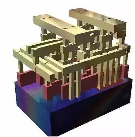
▲ 3D cross-section of an IC chip. (Source: Wikipedia)
From the 3D cross-section of the IC chip shown in the diagram above, the deep blue part at the bottom is the wafer introduced in the previous section. This diagram makes it clearer how important the wafer substrate is in the chip. The red and earth-yellow parts represent the areas to be completed during IC manufacturing.
First, the red part can be likened to the lobby on the first floor of a high-rise building. The lobby serves as the entrance to a building, and since it usually has more functional requirements due to traffic, it is more complex to construct and requires more steps compared to other floors. In the IC circuit, this lobby is the logic gate layer, which is the most important part of the entire IC, combining various logic gates to complete a fully functional IC chip.
The yellow part is like the general floors of a building. Compared to the first floor, it does not have too complex structures, and there will not be too many changes in construction for each floor. The purpose of this layer is to connect the logic gates in the red part together. The reason for needing so many layers is that there are too many lines to connect, and when a single layer cannot accommodate all the lines, multiple layers are needed to achieve this goal. Among them, the lines of different layers will connect up and down to meet the wiring needs.
Layered construction, building up step by step.
After understanding the structure of the IC, the next step is to introduce how to manufacture it. Imagine if you want to create a detailed design using a spray can, you need to first cut out a masking stencil to cover the paper. Then, spray the paint evenly on the paper, and after the paint dries, remove the stencil. By continuously repeating this process, you can complete a neat and complex design. IC manufacturing follows a similar approach, stacking layer by layer using masking.
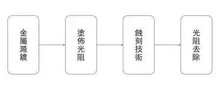
IC manufacturing can be simply divided into the above four steps. Although the actual manufacturing process may vary and the materials used differ, they generally follow similar principles. This process differs from painting in that IC manufacturing involves applying coatings first and then masking, while painting involves masking first and then painting. The following will introduce each process.
Metal Sputtering: Evenly sprinkle the desired metal material on the wafer to form a thin film.
Photoresist Coating: First, place the photoresist material on the wafer, and through a mask (the principle of the mask will be explained next time), shine light on the unwanted parts to destroy the structure of the photoresist material. Then, use chemical agents to wash away the destroyed material.
Etching Technology: Etch the silicon wafer that is not protected by the photoresist using an ion beam.
Photoresist Removal: Use photoresist remover to dissolve the remaining photoresist, thus completing one cycle of the process.
Finally, many IC chips will be completed on a single wafer. The next step is to cut the completed square IC chips and send them to packaging factories for packaging. As for what a packaging factory is, that will be explained later.
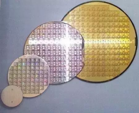
▲ Comparison of various sizes of wafers. (Source: Wikipedia)
What is the nanometer process?
Samsung and TSMC are fiercely competing in advanced semiconductor processes, both trying to seize the initiative in wafer foundry to secure orders, almost resulting in a competition between 14 nanometers and 16 nanometers. However, what do the numbers 14 nanometers and 16 nanometers mean, and which parts do they refer to? What benefits and challenges will come with shrinking the process? Below, we will briefly explain the nanometer process.
How small is a nanometer?
Before starting, we need to understand what a nanometer means. Mathematically, a nanometer is 0.000000001 meters, but this is a rather poor example, as it only shows many zeros after the decimal point without providing a real sense of scale. If we compare it to the thickness of a fingernail, it might be more apparent.
Measuring with a ruler, we find that the thickness of a fingernail is approximately 0.0001 meters (0.1 millimeters), meaning if you try to cut a fingernail’s side into 100,000 lines, each line would be about 1 nanometer, giving a rough idea of how small 1 nanometer is.
After understanding how small a nanometer is, we also need to grasp the purpose of shrinking the process. The main aim of reducing transistor size is to pack more transistors into a smaller chip, preventing the chip from becoming larger due to technological advancements; secondly, it can increase the processing efficiency of the processor; furthermore, reducing size can lower power consumption; finally, a smaller chip can be more easily fit into mobile devices, meeting the future demand for thinner and lighter products.
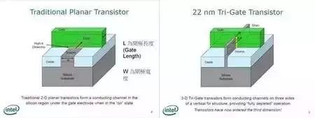
Returning to the nanometer process, taking 14 nanometers as an example, this process refers to the minimum line size that can be achieved in the chip, which can be as small as 14 nanometers. The following diagram shows the appearance of traditional transistors, serving as an example. The main purpose of shrinking transistors is to reduce power consumption, but which parts should be reduced to achieve this goal? The L in the lower left diagram is the part that is expected to be reduced. By reducing the gate length, the current can take a shorter path from the Drain to the Source (if interested, you can search for MOSFET on Google for a more detailed explanation).
 (Source: www.slideshare.net)
Additionally, computers operate using 0s and 1s. How can transistors meet this requirement? The method is to determine whether there is current flowing through the transistor. When a voltage is supplied to the Gate (the green square), current will flow from the Drain to the Source; if no voltage is supplied, current will not flow, thus representing 1 and 0. (For those interested in why we use 0 and 1 for judgment, you can check Boolean algebra; we use this method to create computers).
Size reduction has its physical limits.
However, the process cannot be shrunk indefinitely. When we reduce transistors to around 20 nanometers, we encounter problems from quantum physics that cause transistors to leak, offsetting the benefits gained from reducing L. One way to improve this is to introduce the FinFET (Tri-Gate) concept, as shown in the upper right diagram. According to explanations made by Intel, this technology can reduce leakage phenomena caused by physical phenomena.
(Source: www.slideshare.net)
More importantly, this method increases the contact area between the Gate and the lower layer. In traditional methods (shown in the left upper diagram), the contact surface is only a flat plane, but by adopting FinFET (Tri-Gate) technology, the contact surface becomes three-dimensional, easily increasing the contact area, thus allowing the Source-Drain to become smaller while maintaining the same contact area, which greatly aids in size reduction.
Finally, why do people say that major manufacturers will face significant challenges entering the 10 nanometer process? The main reason is that the size of one atom is about 0.1 nanometers. In the case of 10 nanometers, a line contains less than 100 atoms. This makes manufacturing extremely difficult, and any defect of a single atom, such as an atom falling out during production or the presence of impurities, can lead to unknown phenomena affecting product yield.
If you cannot imagine this difficulty, you can conduct a small experiment. Arrange 100 small beads on a table to form a 10×10 square, then cut a piece of paper to cover the beads, and use a small brush to brush away the beads around it, ultimately forming a 10×5 rectangle. This will give you some idea of the challenges faced by major manufacturers and how daunting it is to achieve this goal.
As Samsung and TSMC recently complete mass production of 14 nanometers and 16 nanometers FinFET, both are vying for Apple’s next-generation iPhone chip foundry. We will see exciting commercial competition and gain more energy-efficient and thinner phones, thanks to the benefits brought by Moore’s Law.
Let me tell you what packaging is.
Packaging is the final protection and integration of IC chips.
After a long process from design to manufacturing, we finally obtain an IC chip. However, a chip is quite small and thin. Without external protection, it can be easily scratched and damaged. Additionally, due to the chip’s small size, it is difficult to place it manually on a circuit board without a larger casing. Therefore, this article will describe and introduce packaging.
Currently, there are two common types of packaging: one is the DIP package, commonly seen in electric toys, resembling a black centipede, and the other is the BGA package, often found when purchasing boxed CPUs. Other packaging methods include the PGA (Pin Grid Array) used in early CPUs or the improved version of DIP, the QFP (Quad Flat Package). Due to the large number of packaging methods, the following will introduce DIP and BGA packaging.
Traditional packaging, enduring through time.
The first to introduce is the Dual Inline Package (DIP). As seen in the following diagram, IC chips using this packaging have dual rows of pins, resembling a black centipede, which leaves a deep impression. This packaging method is the earliest adopted IC packaging technology, with the advantage of low cost, suitable for small chips that do not require many connections. However, since most are made of plastic, the heat dissipation effect is poor, unable to meet the requirements of current high-speed chips. Therefore, those using this packaging are mostly enduring chips, such as the OP741 shown in the diagram, or IC chips that are smaller and require fewer connections.
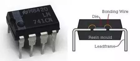 ▲ The IC chip on the left is OP741, a common voltage amplifier. The right image shows its cross-section, where the chip is connected to the metal pins (Leadframe) using gold wire. (Source: Left image Wikipedia, Right image Wikipedia)
As for the Ball Grid Array (BGA) packaging, compared to DIP, the packaging volume is smaller, making it easy to fit into smaller devices. Additionally, since the pins are located at the bottom of the chip, it can accommodate more metal pins compared to DIP, making it suitable for chips requiring more connections. However, this packaging method is more expensive and the connection method is more complex, so it is mostly used in high-priced products.
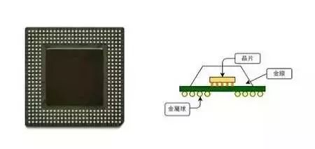 ▲ The left image shows a chip using BGA packaging. The right image is a schematic diagram of BGA with flip chip packaging. (Source: Left image Wikipedia)
The rise of mobile devices, new technologies take the stage.
However, using the above packaging methods consumes a significant amount of volume. Nowadays, mobile devices, wearable devices, etc., require many components. If each component is individually packaged, it will take up a lot of space when assembled. Therefore, there are two methods to meet the requirement of reducing volume, namely SoC (System On Chip) and SiP (System In Package).
When smartphones first emerged, the term SoC could be found in many financial magazines. However, what exactly is SoC? In simple terms, it is the integration of originally different functional ICs into one chip. By doing this, not only can the volume be reduced, but the distance between different ICs can be shortened, enhancing the chip’s computing speed. As for the manufacturing method, it involves placing various ICs together during the IC design phase, then creating a mask through the previously described design process.
However, SoC is not without its drawbacks. Designing an SoC requires considerable technical coordination. When IC chips are individually packaged, each has external protective packaging, and the distance between ICs is relatively far apart, reducing the likelihood of cross-interference. However, when all ICs are packaged together, the nightmare begins. IC design companies must shift from simply designing ICs to understanding and integrating various functional ICs, increasing the workload of engineers. Additionally, there are many situations to consider, such as high-frequency signals from communication chips possibly affecting other functional ICs.
Moreover, SoC also requires obtaining IP (intellectual property) licenses from other manufacturers to incorporate pre-designed components into the SoC. This is because creating an SoC necessitates acquiring the design details of the entire IC to create a complete mask, which also increases the design cost of the SoC. Some may question why not design one themselves? Because designing various ICs requires extensive knowledge related to that IC, only wealthy companies like Apple can afford to hire top engineers from various well-known companies to design an entirely new IC. Collaborating and obtaining licenses is still more cost-effective than developing in-house.
A compromise solution, SiP emerges.
As an alternative, SiP takes the stage in integrated chips. Unlike SoC, it involves purchasing ICs from various manufacturers and packaging them together during the final process, thus eliminating the need for IP licensing, significantly reducing design costs. Additionally, since they are independent ICs, the degree of interference among them is greatly reduced.
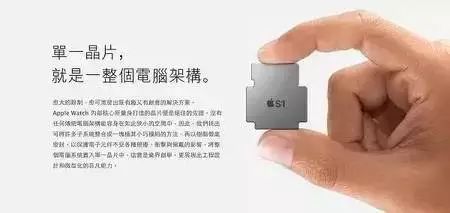 ▲ The Apple Watch uses SiP technology to encapsulate the entire computer architecture into one chip, not only meeting the expected performance but also reducing volume, allowing for more space for the battery. (Source: Apple official website)
Products using SiP technology, the most famous being the Apple Watch. Due to the small internal space of the watch, it cannot adopt traditional technology. The design cost of SoC is too high, making SiP the primary choice. By using SiP technology, not only can the volume be reduced, but the distance between various ICs can be shortened, making it a feasible compromise solution. The following diagram shows the internal configuration of the S1 chip used in the Apple Watch, which contains a considerable number of ICs.
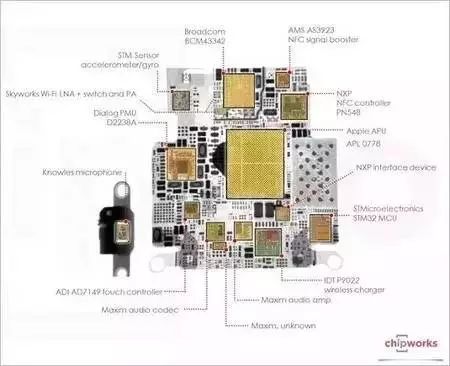 ▲ Internal configuration diagram of the S1 chip using SiP packaging in the Apple Watch. (Source: chipworks)
After completing the packaging, the next step is the testing phase, where we need to confirm whether the packaged IC operates normally. Once confirmed, it can be shipped to assembly plants to create the electronic products we see. Thus, the semiconductor industry completes the entire production task.
Source: Electronic Materials Circle, Copyright belongs to the original author. If there is any infringement, please contact the backstage, and we will handle it as soon as possible.
Recommended Hot Articles
GPCA/SPCA May 2019 Work Brief
[Aiming for a Thousand Miles, Vastness of the Five Continents] Jiangxi Zhihua Production Celebration Successfully Held
[Strategic Layout] Chongda Technology Plans to Invest 210 Million Yuan to Build Chongda Nantong, Focusing on the Semiconductor Field
[Research Report Selection] Pengding Holdings Expects to Invest 3.373 Billion Yuan to Build Headquarters Building, Shenzhen Second Factory, etc.
[Industry Analysis] In the Context of 5G, In-depth Analysis of PCB Industry Development Opportunities
2018 Global Top 30 PCB Manufacturers Overview: Dongshan, Shennan, Jingwang Stand Out
[Layout in Zhuhai] Zicheng Technology’s Annual Output of 450,000 Square Meters of Circuit Board “Intelligent Manufacturing” Factory Project Groundbreaking
[Dialogue with Figures] Shenghong Chairman Chen Tao: Confidence Helps Enterprises Face All Challenges
[Invisible Champion] Hubei Longteng Electronics: An Industry Dark Horse Starting from Charging Interface Circuit Boards
[Signing Agreement] Shangda Electronics Will Build COF/FPC/RFPC Production Base in Suining