The I2C waveform is one of the most common, and today we will directly discuss the diagram.Start Signal: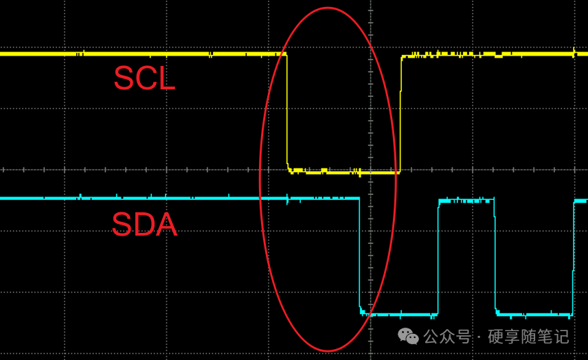 Figure 1Acknowledge Signal:
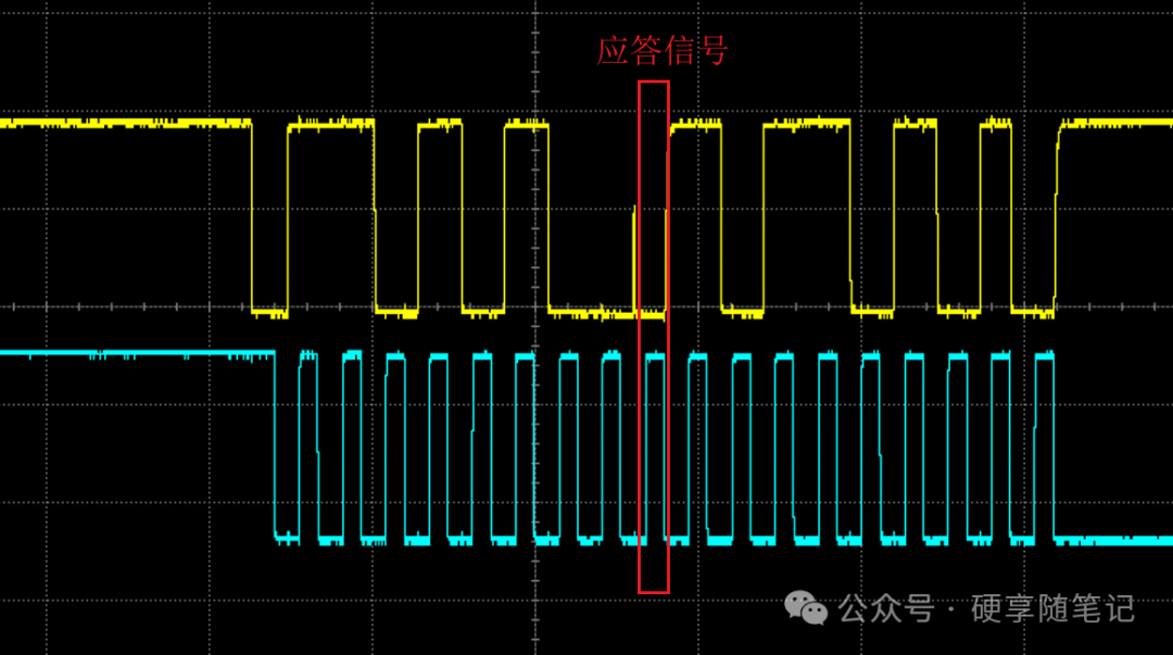 Figure 2Stop Signal:
 Figure 3
 Figure 4Acknowledgment:SACK: acknowledged by slave; the slave device acknowledges the signal, low level indicates received;MACK: acknowledged by master; the master device acknowledges the signal, low level indicates received;NACK: Not acknowledged; the device is unable to receive the next set of data; the appearance of NACK means a stop bit will occur;Read/Write Operations:RW: Read/Write;Write is low level 0; Read is high level 1;Write Timing:
 Figure 5
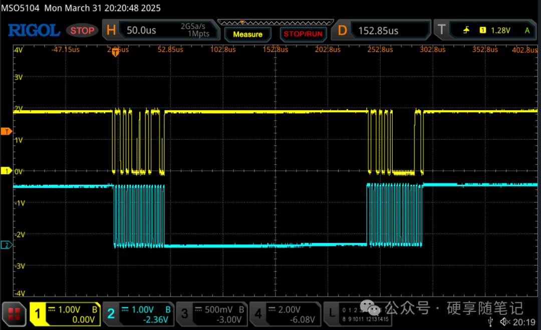 Figure 6Read Timing:
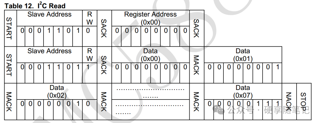 Figure 7Bus Occupation and Release:
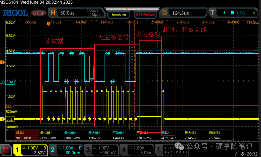 Figure 8Points to Note:1. SCL is always controlled by the Master, and SDA is controlled according to the direction of data transmission. When reading data, the Slave controls SDA; when writing data, the Master controls SDA. After the 8-bit data transmission is complete, the control of the SDA for the acknowledgment or no acknowledgment bit is opposite to that of the data bit transmission. In other words, the level of the acknowledgment bit determines the data direction.2. The Start bit and Stop bit can only be issued by the Master.3. After the 8-bit address transmission is complete, the Slave device that successfully configures the address must send an “ACK”. Otherwise, after a certain time, the Master will consider it a timeout, abandon the data transmission, and send a “Stop”. As shown in the figure.4. When writing data, after the Master sends 8 data bits, if the Slave device has space to accept the next byte, it should respond with “ACK”; if the Slave device does not have space to accept more bytes, it should respond with “NACK”. If the Master receives “NACK” or does not receive any data after a certain time, it will consider it a timeout, abandon the data transmission, and send a “Stop”.5. When reading data, after the Slave device sends 8 data bits, if the Master wishes to continue reading the next byte, the Master should respond with “ACK” to prompt the Slave to prepare the next data. If the Master does not wish to read more bytes, the Master should respond with “NACK” to prompt the Slave device to prepare to receive the Stop signal.6. When the Master is too fast for the Slave to process, the Slave device can pull SCL low (SCL=0 will cause a “line and”) to prevent the Master from sending more data. At this point, the Master will slow down or end the data transmission as needed.In practical applications, there is no strict requirement for the data receiver to respond to the 8 bits of data sent, especially when both the Master and Slave are implemented using GPIO software simulation. The programmer can agree in advance on the length of data transmission, and the Slave does not check for NACK, which can sometimes reduce system overhead. However, if the Slave side is hardware I2C requiring a standard NACK, and the Master side is GPIO software simulating I2C without correctly sending NACK, it will result in the “Slave not receiving Stop” leading to I2C hang.