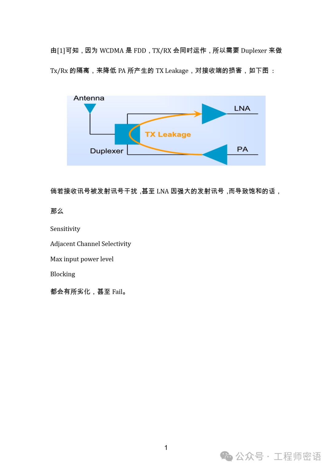
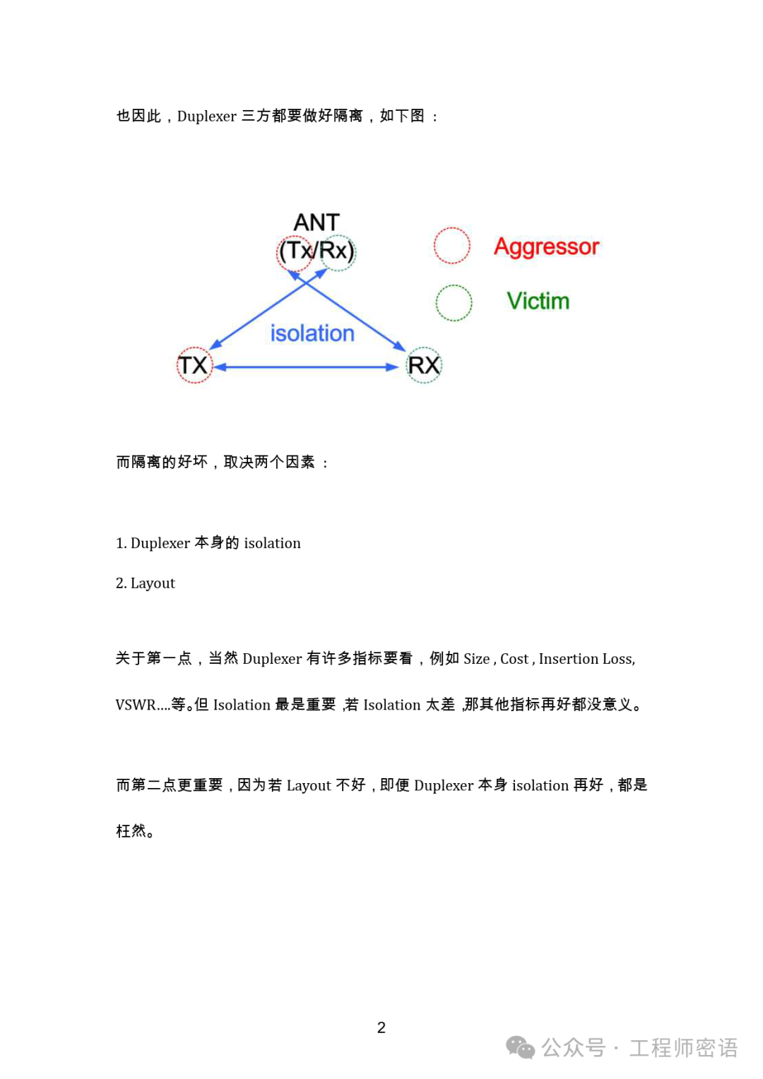
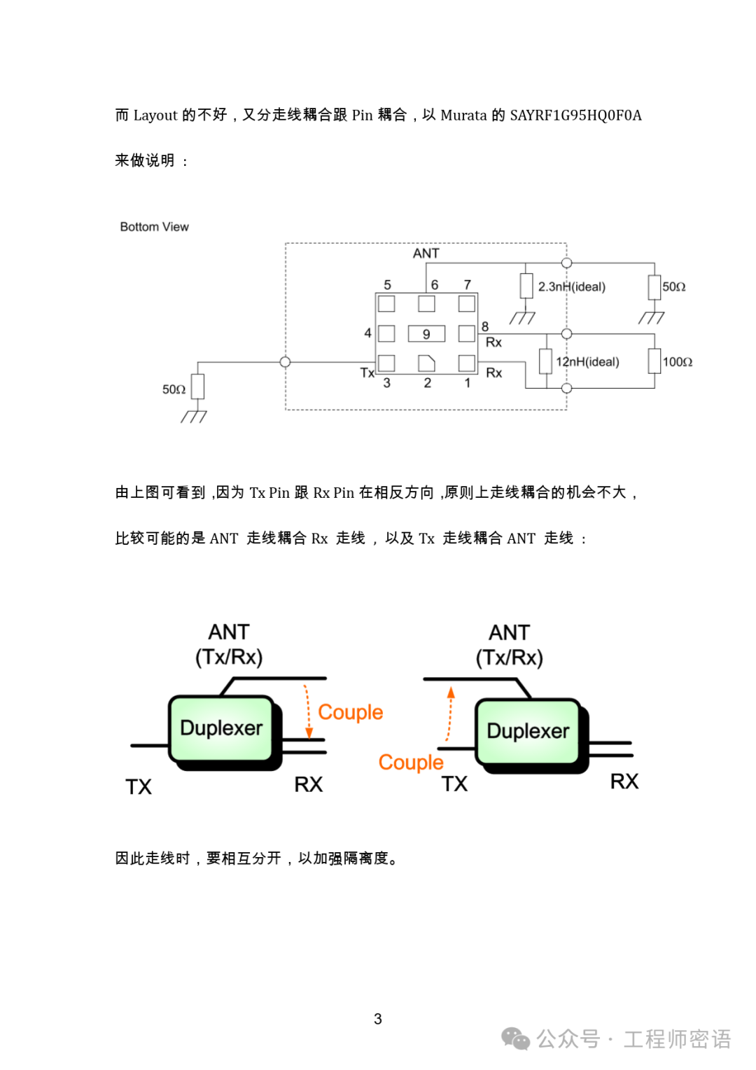
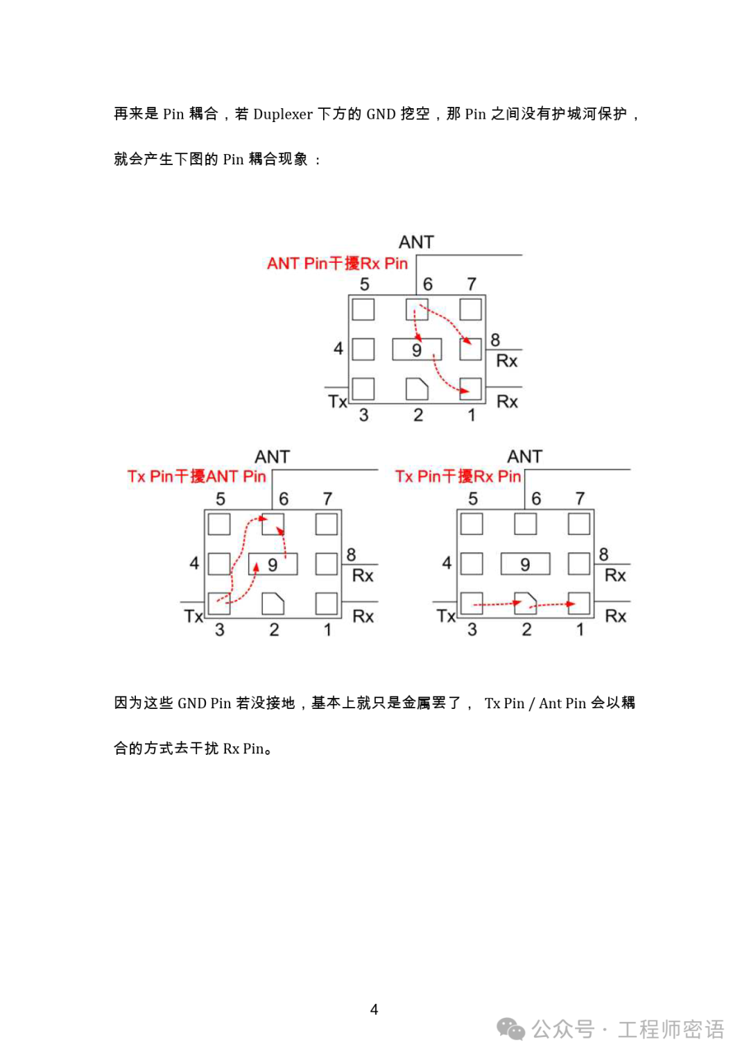
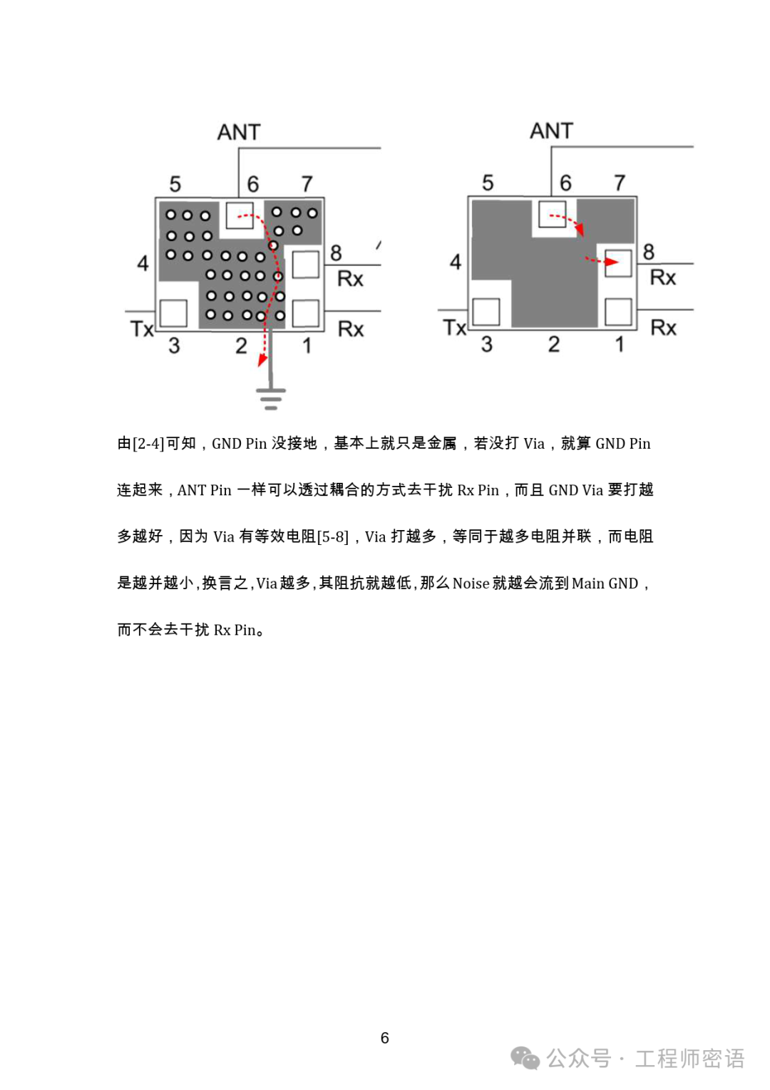
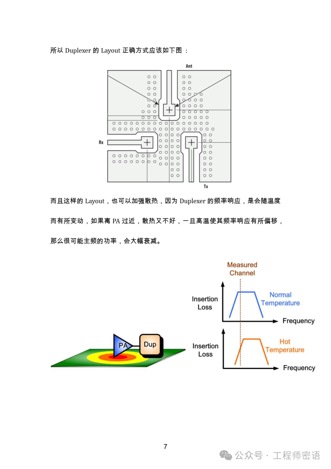
 Summary: In PCB design, the quality of the layout for the duplexer often directly determines the overall RF performance of the device. Many engineers focus more on the positions of major components such as antennas, PA, and LNA, while neglecting the details of the duplexer, which serves as an important intermediate link. In fact, the duplexer is both the boundary between the transmission and reception paths and a crucial safeguard against out-of-band interference. Any improper handling in layout and routing can lead to irreversible performance degradation. First, the layout has a significant impact on isolation. The isolation of the duplexer not only depends on its internal filter structure but is also closely related to parasitic coupling on the PCB. For example, if the traces between the transmission (TX) and reception (RX) ends are parallel and too close together, parasitic capacitance or magnetic coupling may form, causing TX leakage into RX, which can lead to decreased reception sensitivity and worsened EVM. To avoid this situation, ensure that the TX and RX traces are kept at a distance from each other, using ground isolation strips or routing them on different layers to reduce coupling paths. Secondly, grounding design should not be overlooked. The duplexer has very high grounding requirements; any poor grounding can lead to drift in the filter curve or deterioration in the standing wave ratio. It is recommended to place a complete ground copper plane at the bottom of the duplexer and connect it to the main ground plane through dense vias. The distribution of vias should be uniform to avoid the formation of “island” areas, which can easily lead to local resonance at high frequencies, affecting isolation and insertion loss performance. Finally, do not neglect the reverse check during the testing and validation phase. Many designs encounter issues during testing, and tracing the cause often reveals that layout details were not thoroughly considered in advance. It is advisable to use 3D electromagnetic simulation software (such as HFSS, ADS, CST) to perform local simulations of the duplexer and surrounding traces after the design is completed, assessing changes in isolation, insertion loss, and standing wave ratio. Overall, the PCB layout of the duplexer is not a standalone “drawing action” but a system engineering task deeply coupled with the overall RF architecture of the device. A reasonable layout can fully leverage the advantages of the component’s isolation and insertion loss, while an unreasonable design may significantly undermine the performance of the expensive RF front end. As RF engineers, we should treat the layout of the duplexer as a critical design node—not only meeting the reference layout recommended by the component manufacturer but also optimizing it based on the characteristics of the entire board and other practical considerations. Only by meticulously addressing these “details” can we achieve optimal product performance.