Source: Lao Qian and His FriendsOriginal Author: Sun Qian
This article introduces the fundamentals of integrated circuits from atomic structure to transistors.
In the late 19th century, consumer products included simple circuits for lighting, heating, telephones, and telegraphs. However, the invention of radio and the demand for electrical components that could rectify and amplify signals drove the invention of vacuum tubes.Vacuum tubes appeared in products such as radios, televisions, communication devices, and early computers. Their use continued until the late 1960s, when the advent of semiconductor devices ushered in a new era in electronics. The integration of a complex array of transistors and other components on a single integrated circuit (IC) chip improved reliability, reduced power consumption, size, and weight, making today’s advanced electronic products possible.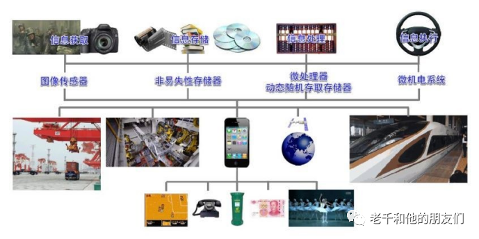 The Impact of Integrated Circuits on Human LifeThe development process from vacuum tubes to integrated circuits has gone through several stages, involving a technological leap from the era of electronic tubes to the era of integrated circuits. The following are the main stages in the development from vacuum tubes to integrated circuits:Vacuum Tube Era (Early to 1950s): Early computers and electronic devices used vacuum tubes as the primary electronic components. A vacuum tube is a device that amplifies electrical signals by controlling the flow of electrons in a vacuum. The use of vacuum tubes was very common in the first half of the 20th century, but they had issues such as being bulky, high power consumption, short lifespan, and fragility.The Invention of the Transistor (1947):The invention of the transistor marked the transition from the era of electronic tubes to the era of semiconductors. In 1947, Joseph R. Lutz and John Bardeen at Bell Labs invented the first transistor. Compared to vacuum tubes, transistors are smaller, consume less power, and have a longer lifespan, which led semiconductor technology to become mainstream in electronic devices.The Concept of Integrated Circuits (1950s-1960s):In 1958, Jack Kilby and Robert Noyce independently proposed the concept of integrated circuits. Kilby manufactured the first practical integrated circuit at Texas Instruments, which contained several transistors and other components.Small-Scale Integration (SSI) and Medium-Scale Integration (MSI) (1960s):In the 1960s, integrated circuit technology began to commercialize, entering the small-scale integration (SSI) and medium-scale integration (MSI) eras. SSI and MSI integrated tens to hundreds of transistors for manufacturing logic gates and simple digital circuits.Large-Scale Integration (LSI) and the Rise of Microprocessors (1970s):In the early 1970s, the introduction of large-scale integration (LSI) technology allowed thousands of transistors to be accommodated on a chip. In 1971, Intel launched the world’s first commercial microprocessor, the Intel 4004, marking the beginning of the microprocessor era.Very-Large-Scale Integration (VLSI) Era (1980s):In the 1980s, the development of very-large-scale integration (VLSI) technology further increased the number of transistors on chips to millions. During this period, the performance of computer chips rapidly improved, and personal computers began to become widespread.Deep Submicron and 3D Integrated Circuits (1990s-Present):In the 1990s, the deep submicron era began, with process technologies further shrinking, enhancing chip performance and integration. In the early 21st century, the introduction of 3D integrated circuit technology allowed multiple functional layers to be stacked vertically on chips, further increasing integration and performance.
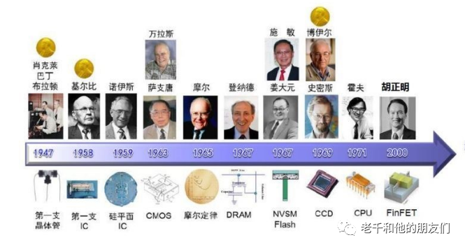 The entire development process reflects the evolution of electronic technology from vacuum tubes to integrated circuits, driving the rapid development of computer science and information technology. The continuous innovation in semiconductor technology has made electronic devices smaller and more powerful, promoting the digital transformation of modern society.To understand integrated circuits, one can start from many angles, such as process technology, application fields, performance indicators, packaging, etc. Here, we will start with the most basic atomic structure.1 Atomic StructureAll matter, whether solid, liquid, or gas, is composed of one or more of the 109 elements discovered in the periodic table. Among these elements, 91 are naturally occurring, while the rest are either man-made or byproducts of other elements. Elements are composed of molecules, which can be further divided into smaller particles called atoms. The atomic structure of each element is different and determines the properties of that element.Materials can be classified based on their conductivity when a voltage is applied. Insulators, as the name suggests, do not conduct electricity, while conductors can allow a large current to flow, depending on the voltage applied and the material’s conductivity. Semiconductors have properties between conductors and insulators, allowing a limited current to flow, where the current size depends on the atomic structure, material purity, and temperature.Atoms consist of a highly dense nucleus made up of protons and neutrons, with negatively charged electrons rotating around it in specific orbits (or energy levels). This structure was first proposed by Neils Bohr in 1913 and has since received substantial experimental support. Protons carry a positive charge, while neutrons are neutral, thus maintaining electrical neutrality. Each atom has an equal number of protons (+) and electrons (-), while the number of neutrons can vary.Each element in the periodic table has an atomic number equal to the number of protons, and thus also equal to the number of electrons in its atom. The atomic number is indicated at the top of each element.
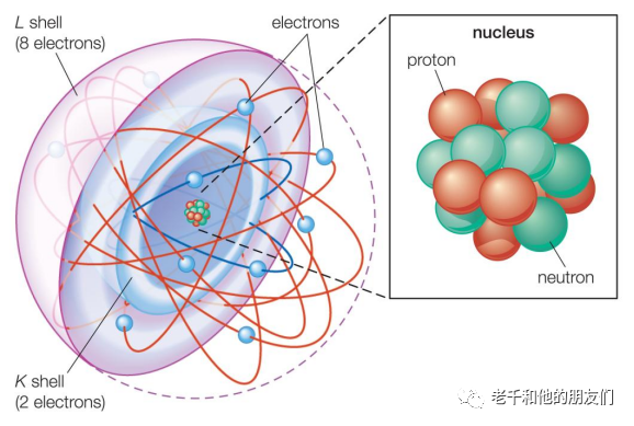 Figure 1 Atomic Structure Model: Atoms are composed of protons, neutrons, and electrons, with protons and neutrons forming the nucleus, and electrons orbiting around the nucleus.The actual mass of an atom is extremely small, making its study very difficult. Therefore, a specific unit of mass is defined to represent the mass of atoms, indicating the mass of one atom relative to another. This mass unit is based on the sum of protons and neutrons in the densest part of the atom, namely the nucleus.The positively charged protons exert a centripetal force on the negatively charged electrons, which is balanced by the outward centrifugal force produced by the spinning electrons in the atom’s orbits. Thus, these two opposing forces provide a balanced structure for the atom. The maximum number of electrons that can occupy a given orbit or shell follows the 2n² rule, where ‘n’ is the shell number.If the number of electrons in a given shell exceeds the maximum number given by the 2n² rule, the excess electrons will be forced into the next higher shell. If the outer shell of an atom is completely filled according to the 2n² rule or contains 8 electrons, it is chemically stable. The electrons in the outer shell are called valence electrons, and if their number is less than 8, the atom tends to either lose or gain electrons or share electrons with other atoms to interact with them.Elements in the periodic table with the same number of valence electrons exhibit similar properties and are placed in the same group. For example, group IA elements have 1 electron in their outer shell, while group IIA elements have 2 electrons in their outer shell. Elements on the left side of the periodic table tend to lose valence electrons to other atoms, thus becoming positively charged. Elements on the right side of the periodic table tend to gain electrons from other atoms, becoming negatively charged.
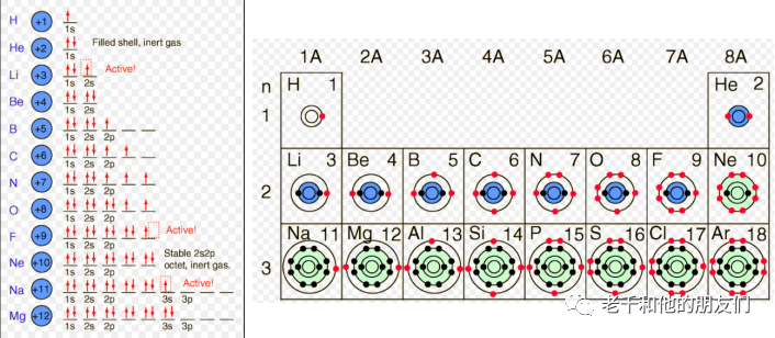 Figure 2 The Orbits and Electron Capacity of the First Four Principal Energy LevelsWhen atoms come close to each other, the type of interaction that occurs mainly depends on the properties of the atoms themselves.This interaction forms what is called a chemical bond, which can be classified into ionic bonds, covalent bonds, molecular bonds, hydrogen bonds, or metallic bonds.A covalent bond is formed when two or more atoms share their valence electrons. If the outer shell is only partially filled with electrons, the atom will be attracted to other atoms that are missing electrons, so sharing their valence electrons can lead to a more stable state. For example, two chlorine atoms will attract and share their single electrons, forming a stable covalent bond with 8 electrons in each shell.2 Vacuum TubesModern electronics can trace its roots back to the first electronic device called the vacuum tube. Although solid-state devices have almost completely replaced vacuum tubes today, their basic principles have not changed much in terms of functionality. For over 40 years, until the late 1960s, the most important components of consumer electronic products were still vacuum tubes.The vacuum tube was invented in 1883 when Edison created the incandescent lamp. To improve the problem of the filament burning out too early, he conducted many experiments, one of which involved sealing a metal plate inside the bulb and connecting it to a battery and ammeter.Edison observed that when the filament was heated and the metal plate was connected to the positive terminal of the battery, the ammeter indicated that current passed through the vacuum gap between the filament and the metal plate. When the metal plate was connected to the negative terminal of the battery, the current stopped flowing. Although this phenomenon was significant, it did not improve the lifespan of Edison’s bulb, so he lost interest in this experiment and turned to other research that could more successfully improve the bulb.For the next twenty years, Edison’s vacuum tube experiment remained a focus of the scientific community. In 1903, as radios began to be used, J.A. Fleming in England discovered that he needed something to rectify alternating radio signals into a direct current signal needed for headphones. He connected Edison’s vacuum tube to the receiving antenna, and the vacuum tube worked like a diode. When the signal voltage increased in one direction, it made the metal plate positive, allowing the signal to pass; when the signal voltage increased in the other direction of the alternating cycle, it applied a negative charge to the metal plate, stopping the signal.A vacuum tube, also known as an electronic tube, requires a source of electrons to operate. In Edison’s original electronic tube, the source of electrons was the filament, called the cathode. When heated to red-hot, the filament emitted electrons toward the positively charged metal plate in the vacuum, which is called the anode. The process of heating the cathode to activate the electrons is known as the thermionic emission effect. Other types of electronic tubes use high voltage to pull electrons from a cold cathode.
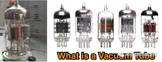 Figure 3 Vacuum DiodeApplying light energy to a photo-sensitive cathode can also result in the emission of electrons. Vacuum tubes that utilize this effect are called photoelectric vacuum tubes. Although there are various methods to remove electrons from the cathode, thermionic vacuum tubes are the most widely used. The cathode can be heated either by its inherent resistance or by using a separate power source. A vacuum tube consists of a glass or metal bulb with electrode leads, and the electrode leads are drawn through the glass and connected to metal pins molded in a plastic tube base.When a vacuum tube contains two electrodes (anode and cathode), this circuit is called a diode. In 1906, American inventor Lee DeForest added a gate (a fine metal mesh) between the cathode and anode. The addition of the third electrode expanded the applications of vacuum tubes to other electronic functions. The gate provides a method to control the flow of electrons from the cathode to the metal plate (anode); although the gate has a small positive or negative charge, being close to the cathode greatly influences the flow of electrons from the cathode to the anode.
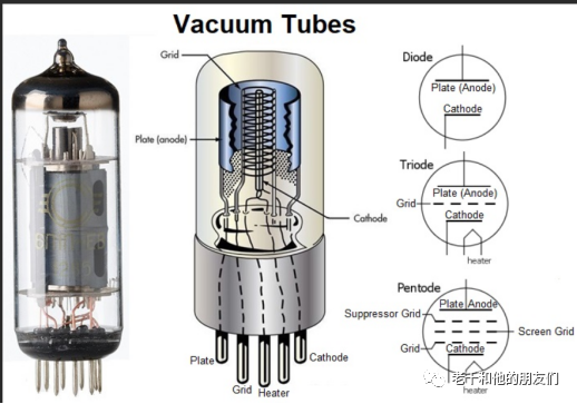 Figure 4 The Gate Controls the Flow of Electrons to the Triode PlateA sparsely woven gate can allow most electrons to pass through and fall onto the positively charged anode. When the gate is negatively charged, it repels electrons from the cathode, stopping the flow of current.Thus, in the case of three electrodes (i.e., cathode, anode, and gate), a vacuum tube can be used to rectify and amplify weak radio signals. A vacuum tube with three electrodes is called a triode; more electrodes, such as suppressor gates and screen grids, can also be sealed in the electronic tube to expand its functionality.Despite being widely used in industry for over half a century, vacuum tubes have many disadvantages, including being bulky, generating significant heat, and being prone to damage, requiring frequent replacements. Advances in solid-state devices have eliminated the drawbacks of vacuum tubes, leading to their gradual withdrawal from many electronic products.3 Semiconductor TheorySemiconductor materials have physical properties that are completely different from metals. Metals can conduct electricity at all temperatures, while semiconductors conduct better at certain temperatures and poorly at others. Semiconductors are covalent solids, meaning that the atoms themselves form covalent bonds. The most important semiconductor elements are silicon and germanium from group IVA of the periodic table. If two or more elements form covalent bonds, they can also form semiconductor compounds, such as gallium (group IIIA) and arsenic (group VA) combining to form gallium arsenide.Typical semiconductor materials used in IC chip manufacturing include the following: elemental semiconductors: silicon; germanium; selenium. Semiconductor compounds: gallium arsenide (GaAs); phosphide gallium (GaAsP); indium phosphide (InP).Germanium was used to manufacture the first transistor and solid-state devices. However, due to its difficulty in processing and limited device performance, it is now used less frequently. Another elemental semiconductor is silicon, which is used to manufacture about 90% of chips. The widespread use of silicon is related to its abundant resources in nature and its ability to maintain good electrical performance at high temperatures. Additionally, silicon oxide (SiO2) has many ideal properties suitable for IC manufacturing.Gallium arsenide belongs to compound semiconductors. Its certain properties, such as higher operating frequency (2-3 times higher than silicon), low thermal dissipation, radiation resistance, and minimal leakage between adjacent components, make gallium arsenide an important semiconductor for high-performance applications. Its disadvantage is the difficulty in crystal growth and IC manufacturing.A semiconductor or compound semiconductor that is free from impurity contamination is called an intrinsic semiconductor. At absolute zero temperature, intrinsic semiconductors form stable covalent bonds, and their valence electron shells are completely filled with electrons, making these covalent bonds very strong, thus binding each electron strongly to its atom. Therefore, there are no remaining free electrons, and it cannot conduct electricity. As the temperature rises, the valence band tends to break, releasing electrons. The behavior of these free electrons is similar to that of free electrons in metals, allowing conduction when an external electric field is applied.If an impurity, such as phosphorus or boron, is introduced into the crystal structure of an intrinsic semiconductor, the semiconductor’s chemical state will change to a semiconductor with excess electrons or a lack of electrons, depending on the type of impurity used. The process of adding a small amount of impurity to an intrinsic semiconductor is called doping.Taking an intrinsic silicon crystal structure with covalent bonds as an example: each atom has four other atoms with which it shares a pair of electrons, forming four covalent bonds. If a controllable amount of impurity (dopant) such as phosphorus (group VA) is doped into the silicon crystal (group IVA), the newly formed covalent bonds will have excess electrons. When voltage is applied to the semiconductor, these electrons can move freely from one atom to another. The material that has been altered in this way is called n-type (n for negative) semiconductor; another type of semiconductor called p-type (p for positive) is formed by doping silicon crystal with a group IVA dopant such as boron. The resulting semiconductor lacks electrons, creating “holes” in the positively charged atoms, which are vacancies where electrons are absent.A single semiconductor crystal structure can be selectively doped with two different types of impurities, forming adjacent p-type and n-type semiconductors. The transition region between the two semiconductors is called a p-n junction, where electrons and holes recombine. When electrons enter the p-type region, they fill the holes, making the atoms negatively charged, while the remaining atoms with fewer electrons become positively charged, creating new holes (this process can be viewed as the flow of holes or the flow of positive vacancies, which is opposite to the direction of electron flow). Due to the depletion of electrons and holes in the contact region, the p-n junction is called a depletion region. An electric field is established between the layers of atoms with two different charges on either side of the contact region, preventing further recombination of electrons and holes in this area, forming a barrier layer.
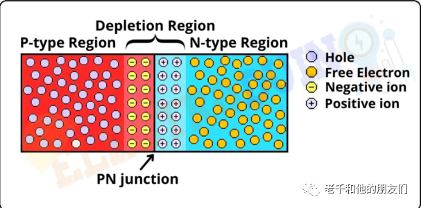 Figure 5 p-type/n-type Semiconductor Junction and p-type/n-type Semiconductor Junction with Depletion Region4 DiodesWhen an external battery is placed across the p-n junction, with the positive terminal connected to the n-type side of the semiconductor and the negative terminal connected to the p-type side, a so-called reverse bias is formed across the junction. When electrons are attracted to the positive terminal of the battery and holes are attracted to the negative terminal, electrons and holes run away from the junction, increasing the depletion region and preventing current flow.
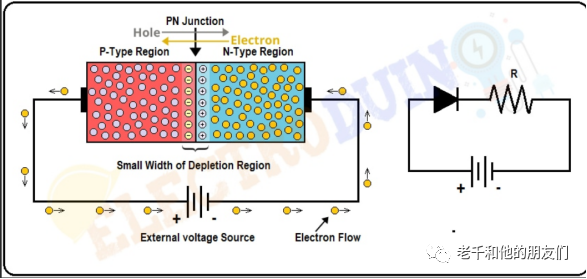 Figure 6 PN Junction Diode Forward BiasIf the battery’s terminals are reversed, the electrons in the n-type semiconductor and the holes in the p-type semiconductor move towards the junction due to repulsion from the negative and positive potentials of the battery, respectively. This reduces the barrier effect of the junction, allowing electrons and holes to pass through and recombine.When electrons and holes recombine, new electrons from the battery (terminal A) enter the n-type region, replacing the electrons that crossed to the p-type region. Similarly, the electrons in the p-type region are attracted to the (+) terminal, leaving new holes that are filled by electrons from the n-type region. This continuous recombination process establishes a forward current across the junction, known as forward bias. Thus, the junction acts as a diode (rectifier), allowing current to flow when the junction is forward biased, and stopping current when reverse biased.5 Bipolar Junction TransistorsCombining two or more p-n junctions into a single device (p-n-p, n-p-n, etc.) leads to the emergence of transistors. A transistor is a device capable of amplifying signals or switching currents billions of times per second, marking a new era in electronics.Since the invention of the transistor by W. Shockley, J. Bardeen, and W. Brattain at Bell Labs in 1948, transistors have developed into many forms. The initial devices used point-contact to penetrate germanium semiconductor material. The subsequent transistors were made using the junction (bipolar) type of semiconductor, with germanium later replaced by silicon.To illustrate how bipolar transistors work, consider the n-p-n semiconductor structure as an example. In this structure, a thin lightly doped p-type region called the base (B) is sandwiched between two thicker n-type regions called the emitter (E) and collector (C). Their leads are referred to as the base, emitter, and collector. The emitter generates electrons, while the collector absorbs them, with the input signal applied to the base controlling the flow of electrons from the emitter to the collector.
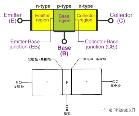 Figure 7 Typical n-p-n TransistorFigure 8 shows a typical circuit of a bipolar transistor used as a digital switch. A voltage Vce is applied between the emitter and collector, with the positive terminal of the power supply (+) connected through a load resistor R to the collector lead. A positive voltage Vbe > 0.5V is applied between the base and emitter leads to turn on the transistor.Since the emitter-base junction is forward biased, the electrons in the emitter will cross the junction into the base region, where some of the electrons will recombine with holes in the lightly doped base region. Because the base region is thin, free electrons are close to the collector, and these electrons are influenced by the positive potential of the collector, crossing the collector-base junction and continuing to flow through the external circuit. Reducing the input voltage to zero will stop the flow of electrons across the emitter-base junction, turning off the transistor.When a bipolar transistor is used as an amplifier, the current flowing from the emitter to the collector is related to the intensity of the input voltage, but the current is amplified. In other words, increasing the intensity of the input voltage at the base will proportionally cause more electrons to cross the emitter-base junction, thus increasing the current flowing between the emitter and collector. Decreasing the input voltage will reduce the speed at which electrons cross the emitter-base junction, thereby decreasing the current. Since bipolar transistors can amplify both current and voltage equivalently, they can also be considered power amplifiers.The characteristic of bipolar transistors is their high-frequency response capability, equivalent to a very high switching speed. However, to achieve very high switching speeds, the transistor must operate at very high currents flowing from the emitter to the collector, which increases power loss.
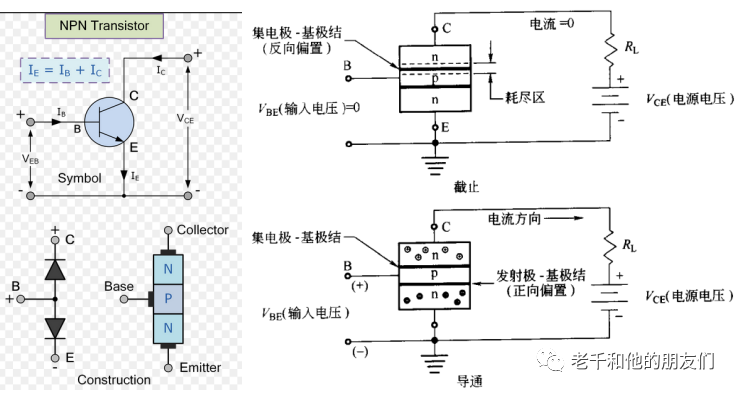 Figure 8 Bipolar Transistor Used as a Digital Switch6 Field Effect TransistorsField Effect Transistors (FETs) operate on different principles than bipolar transistors. The input voltage creates an electric field that changes the resistance of the output region, thereby controlling the flow of current. Its uniqueness lies in its high input resistance, which prevents the load on its preceding devices from dropping, as a reduced load would degrade its performance.The working principle of FETs was known long before the development of bipolar transistors, but due to manufacturing difficulties, people preferred bipolar transistors over FETs.In the 1960s, after solving early manufacturing issues, interest in FETs was reignited. FETs, like bipolar transistors, also have three semiconductor regions, but due to the difference in working principles, the three regions in FETs are called the source, drain, and gate (if we again consider the n-p-n structure, both the source and drain are n-type semiconductors, while the gate is a p-type semiconductor). There are two types of FETs: Junction Field Effect Transistors (JFETs) and Metal-Oxide-Semiconductor Field Effect Transistors (MOSFETs).6.1 Junction Field Effect TransistorsIn Junction Field Effect Transistors (JFETs), electrons do not cross the P-N junction; instead, they flow from the source to the drain through a so-called n-channel formed between two p-type semiconductors, with the n-channel serving as the output part of the transistor, while the gate to source P-N junction is the input part. In a typical JFET circuit functioning as a digital switch, a power supply voltage VSD is applied across the source (-) and drain (+) terminals through a load resistor Rl, while an input voltage VGS is connected between the gate and source terminals, with the gate connected to a negative terminal.When the input voltage is reverse biased, the electric field creates a depletion region around the p-n junction characterized by a lack of electrons. As the input voltage increases, the depletion region penetrates deeper into the channel, limiting the flow of electrons between the source and drain.If the input voltage is high enough to completely fill the depletion region, the flow of electrons will be interrupted. Reducing the input voltage Vgs to zero will eliminate the depletion region, fully opening the n-channel, resulting in very low resistance, allowing the maximum flow rate of current. When JFETs are used as linear amplifiers, changes in the input voltage will have a corresponding effect on the flow of current within the n-channel, resulting in gain in the output voltage between the source and drain terminals.
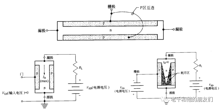 Figure 9 When the p-n junction is forward biased, the JFET functions as a closed switch; when the p-n junction is reverse biased, the JFET functions as an open switch.6.2 Metal-Oxide-Semiconductor Field Effect TransistorsAnother type of FET is the Metal-Oxide-Semiconductor Field Effect Transistor (MOSFET). It operates on the same principle as JFETs but uses the input voltage applied across the built-in capacitor to control the flow of electrons from the source to the drain.MOSFETs generally consist of a source and drain (n-type region) embedded in a p-type semiconductor. Their gate terminal is connected to a metal (aluminum) layer, which is insulated from the p-type semiconductor by a silicon dioxide (SiO2) insulator. This combination of metal, silicon dioxide (insulator), and p-type semiconductor forms a decoupling capacitor. The gate region is located between the source and drain, with a fourth region called the substrate beneath the gate. The substrate can either be connected to the source region or serve as an external terminal.
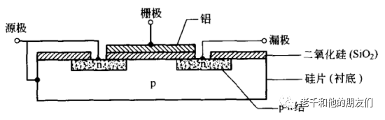 Figure 10 Typical Structure of a MOSFET (Metal-Oxide-Semiconductor Field Effect Transistor)The flow of electrons from the source to the drain is controlled by the gate, regardless of whether the gate has a positive or negative voltage. If the input voltage applied to the gate is positive, free electrons will be attracted from the n-region and p-region to the underside of the gate region’s silicon dioxide layer. The accumulation of electrons beneath the gate forms an n-channel between the two n-regions, providing a conductive path for current to flow from the source to the drain. In this case, the MOSFET is turned on. If the input voltage at the gate is negative, the electrons in the p-region beneath the gate are repelled, preventing the formation of a channel. Since the resistance in the p-region between the two n-regions is infinitely large, no current will flow, and thus the MOSFET is turned off. The MOSFET described above is n-p-n type, but p-n-p type MOSFETs can also be constructed, though their voltage polarity will be reversed.
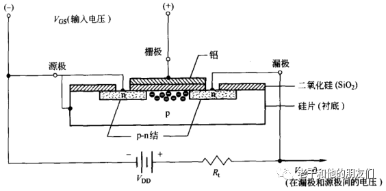 Figure 11 The Function of the MOSFET is to Act as an “On” Switch6.3 Complementary Metal-Oxide-Semiconductor Field Effect TransistorsWhen two MOSFETs (one n-p-n type and the other p-n-p type) are connected together, this combined structure is called a Complementary MOSFET or Complementary Metal-Oxide-Semiconductor Field Effect Transistor (CMOSFET). The advantages of CMOSFET transistors include simplifying circuits (no load resistors needed), very low power dissipation, and the ability to produce an output signal that is inverted relative to the input signal. For example, a positive input will yield a zero output, or a zero input will produce a positive output.
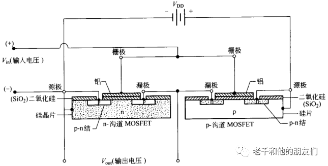 Figure 12 CMOSFET (n-p-n MOSFET and p-n-p MOSFET Connected to Form a Switch)CMOSFET (also known as CMOS transistor) stands for Complementary Metal-Oxide-Semiconductor Field-Effect Transistor, and it is the most common type of transistor used in integrated circuits. In integrated circuit technology, CMOSFETs are widely used in digital circuits and microprocessors.In addition to CMOSFETs, there are several other important technologies and developments, such as:FinFET Technology:FinFET is a three-dimensional transistor structure that replaces traditional planar transistors.Advanced Process Technology:With continuous technological advancements, integrated circuit manufacturing has adopted increasingly advanced process technologies. This includes process levels of 7nm, 5nm, 3nm, etc. Advanced process technology can improve integration, reduce power consumption, and enhance performance.Quantum Dot Technology:Quantum dots are nanoscale semiconductor particles that can be used in optoelectronics and quantum computing. In integrated circuits, quantum dot technology can be applied to light-emitting diodes (LEDs) and display technologies.3D Integrated Circuits:3D integrated circuits are a technology that stacks multiple chip layers vertically. This method can increase integration, reduce the distance for electronic signal transmission, thereby enhancing performance and reducing power consumption.Optoelectronic Integrated Circuits:Optoelectronic integrated circuits are electronic circuits that integrate optical components. This technology aims to use optical signals rather than electrical signals to transmit information, potentially increasing transmission speed and reducing power consumption.Spintronics:Spintronics is a new type of electronics technology based on electron spin rather than electron charge. Research in this field aims to utilize spin for information storage and processing.Quantum Computing:Quantum computing is a computing technology based on quantum bits. Unlike traditional bits (0 and 1), quantum bits (qubits) can exist in multiple states simultaneously, giving quantum computing great potential advantages for certain problems.These technologies and developments represent the cutting edge of research and innovation in the field of integrated circuits. With continuous technological advancement, more new technologies will emerge in the future, driving the development of integrated circuits.
END
Reprinted content only represents the author’s views.
It does not represent the position of the Institute of Semiconductors, Chinese Academy of Sciences.
Editor: Xiao Shuai
Editor-in-chief: Mu Xin
Submission Email: [email protected]
Previous Recommendations
1. The Semiconductor Institute has made progress in the research of bionic covering neuron models and learning methods.
2. The Semiconductor Institute has made significant progress in inverted structure perovskite solar cells.
3. Why is copper used as the interconnect metal in chips?
4. What exactly is 7nm in chips?
5. Silicon-based integrated photonic quantum chip technology.
6. How anomalous is the quantum anomalous Hall effect? It may bring about the next revolution in information technology!