Introduction
Why Should We Understand Both Hardware and Software?
In 2010, while I was at Huawei, I temporarily took a break from my regular duties to participate in recruitment efforts. To recruit more people for my department and compete for HC numbers (the number of positions available), I worked hard to ensure that every candidate who met the strict criteria could pass through the multiple interview stages.
How Huawei Develops (21) – Interviews
During Huawei’s recruitment process, there are many strict requirements for lower-level positions, such as: the school must meet certain standards, candidates should not frequently change jobs, must not have repeated years, and must pass technical interviews, group interviews, and psychological assessments, ultimately being sent to the final interview panel for the final decision; then sent for human resources review and headquarters approval.
We train recruitment personnel, and to complete recruitment tasks, we often relax technical interview standards, guide group interviews, and provide hints during psychological assessments; we strive to send candidates who meet the school requirements to the final interview.
Once, while in Qingdao, very few candidates passed the interview that day. Finally, we found a candidate from a school that barely met the requirements, but their technical skills were lacking. We relaxed our standards all the way. Ultimately, we sent him to the department head for the final interview.
Shortly after, the department head came out and said to me, “Let him go…”.
After I sent the candidate away, I asked the head, “That candidate met all the strict requirements, why was he rejected?”

The head took a drag from his cigarette and said to me, “A person who has been working with microcontrollers for three years, only knows how to draw circuits but cannot write code… One, their learning ability is weak; two, they are hard to teach; three, their existing skill base is too weak. Even if we hire them, they will only be able to draw circuits, but the complexity of the circuits is much greater than that of a simple microcontroller system. Someone who can only draw MCU circuits and doesn’t know how to learn coding must be at a very low level. We don’t want them!”
At that time, I didn’t understand and thought the leader was being arbitrary in his choices, not considering the hard work we put into recruitment. The next day in Jinan, the head told me, “These people we recruit will be your subordinates, and if they are hard to train, it will only cause you trouble.”
However, looking back now, I think there is some truth to that.
Classic Article on Balancing Hardware and Software
Through this article, we will look at the entire process of GPIO initialization and operation from the internal principles of the chip, circuit design, software development, and software operation. This will help many friends who only do MCU hardware and want to improve their understanding.
1. Familiarize Yourself with the Internal Structure and Working Principles of the Chip
For any development, we should first look at the manufacturer’s datasheet and design references; other textbooks, documents, books, websites, and blogs are all based on the original manufacturer’s materials.
Therefore, we should download and carefully read the following two documents:
https://www.st.com/resource/en/datasheet/cd00191185.pdf
http://www.st.com/stonline/products/literature/rm/13902.pdf
The above two links can be copied to your computer for download.
You can also download them from the iBox section of the Hard Ten forum:
http://www.hw100k.com/forum.php?mod=viewthread&tid=3511&extra=
STM32 Physical Diagram:
Of the 144 pins on the STM32, aside from the power, GND, clock, and reset pins that supply power to the chip, almost all pins can be used as GPIO.
2. STM32 LQFP144PIN Pin Distribution Diagram:
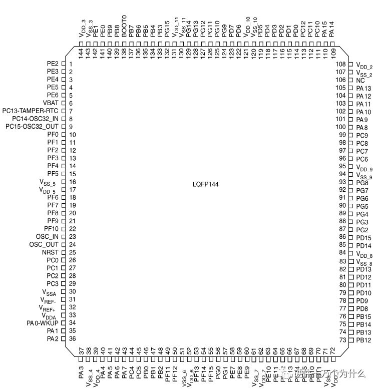
STM32F103ZET6: A total of 144 pins, 7 groups of IO ports, each group has 16 IO ports
7*16=112 IO ports (These 7 groups of IO ports are GPIOA, GPIOB… GPIOG)
For example: PGIOA includes PA0, PA1, PA2… PA15, each group has 16 IO ports.
From the hardware perspective, they are divided into 7 groups: A, B, C, D, E, F, G.
Each group has 16 pins.
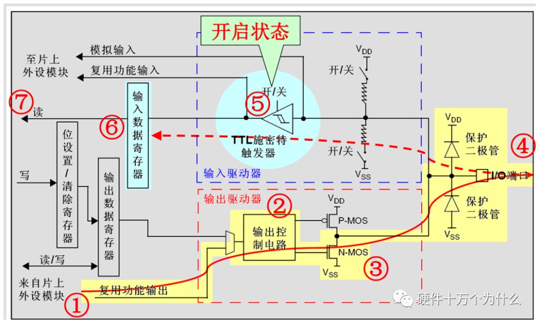
Basic Structure and Working Method of IO Ports

The configuration modes of STM32’s GPIO include several types:
4 Input Modes
Input Floating
Input Pull-Up
Input Pull-Down
Analog Input
4 Output Modes
Open-Drain Output
Open-Drain Multiplexed Function
Push-Pull Output
Push-Pull Multiplexed Function
Configurable Maximum Toggle Speeds of 3 Types
2MHz
10MHz
50MHz
1. Analog Input;
Some pins can be used as ADC input pins and need to be configured through software.
When we configure the corresponding GPIO as ADC functionality.

The signal connected to the GPIO pin will be detected by the ADC integrated within the MCU.
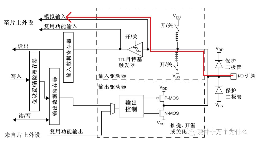
From the above diagram, we can see that the most important point about analog input is that it does not go through the input data register, so we cannot obtain the analog input value by reading the input data register. This is easy to understand because the input data register only stores 0 or 1, while the analog input signal does not meet this requirement, so it cannot be stored in the input data register. This input mode allows us to obtain external analog signals.

If the signal is not used as an analog input, it can be used as a digital signal input.
When using digital signal input, pull-up and pull-down resistors can be configured: high impedance state, no pull-up or pull-down, for floating input.
If the pull-up resistor is enabled, it will be a pull-up input; if the pull-down resistor is enabled, it will be a pull-down input.
Both pull-up and pull-down are in the off state (AD conversion – converting analog to digital)
The Schmitt trigger is in the cutoff state
Input to the CPU through the analog input channel
External voltage at the IO port is an analog quantity (voltage form, not level form), with a typical analog input range of 0~3.3V
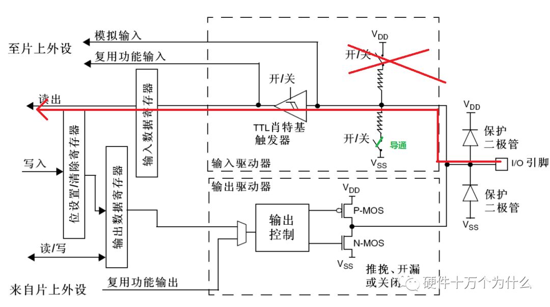
2. Floating Input;
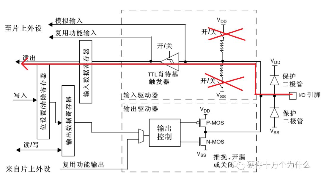
In this input state, my understanding is that the input is entirely determined by external factors. I believe this mode can be used in data communication. In data communication, we intuitively understand that the two ends of the line are connected to the sender and receiver, and they both need to accurately receive each other’s signal levels without external interference. Therefore, I think this situation is suitable for floating input, such as the input state in I2C communication.

1) External input level through IO port, external level passes through the pull-up/pull-down section (both are off in floating mode, meaning no pull-up or pull-down resistors)
2) Transmitted to the Schmitt trigger (at this time, the Schmitt trigger is in the on state)
3) Continue to transmit to the input data register IDR
4) The CPU reads the external input level value through the input data register IDR. In floating input mode, the external input level can be read.
3. Pull-Up Input;
Pull-up input means that a pull-up resistor is used in the input circuit. The advantage of this mode is that when we do not input anything, due to the internal pull-up resistor, our processor will think we have input a high level, thus avoiding uncertain inputs. This is very useful when the input level only needs to be high or low.
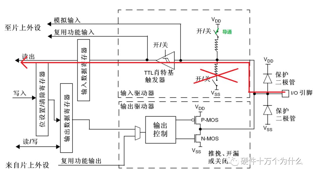
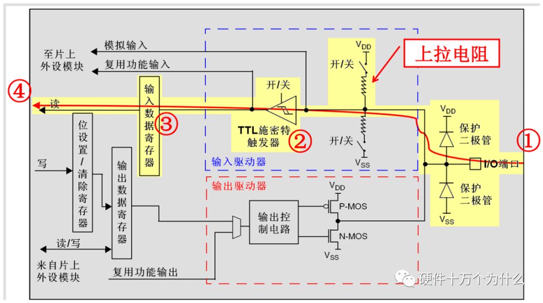
Compared to floating input mode, the difference is that there is an internal pull-up resistor connected to VDD (in pull-up input mode, the pull-up resistor switch is on, with a resistance value of about 30-50K)
External input passes through the pull-up resistor, the Schmitt trigger stores it in the input data register IDR, which is read by the CPU.
4. Pull-Down Input;
Similar to pull-up input, but in pull-down input, when there is no external input, our processor will think we have input a low level.
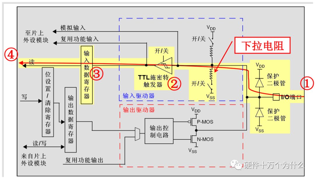
Compared to floating input mode, the difference is that there is an internal pull-down resistor connected to VSS (in pull-down input mode, the pull-down resistor switch is on, with a resistance value of about 30-50K)
External input passes through the pull-down resistor, the Schmitt trigger stores it in the input data register IDR, which is read by the CPU.
5. Open-Drain Output;
Open-drain output means that the output terminal is equivalent to the collector of a transistor, so it is suitable for applications that require current driving. To achieve a high level, a pull-up resistor is needed (for example, to implement I2C output in simulation software).

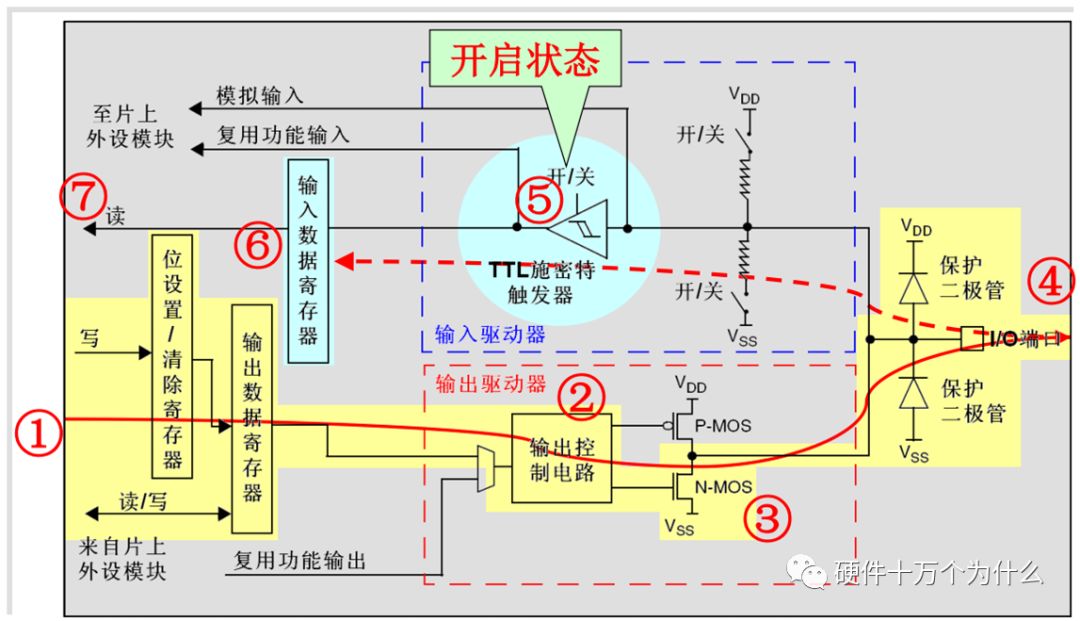
1. The CPU writes to the bit set/reset register BSRR, which maps to the output data register ODR
2. Connect to the output control circuit (which is the level of ODR)
3. The ODR level enters the N-MOS transistor through the output control circuit
– ODR output 1:
N-MOS is off, the IO port level will not be determined by ODR output, but by external pull-up/pull-down.
In the output state, the output level can be read, and the data is stored in the input data register, which can be read by the CPU, allowing the CPU to read the output level.
So, when N-MOS is off, if the output level read is 1, it does not necessarily mean we output 1; it could be 1 generated by the external pull-up.
– ODR output 0:
N-MOS is on, the IO port level is pulled down to VSS, making the IO output low level.
At this time, the low output level can also be read by the CPU.
6. Push-Pull Output;
Push-pull output uses a push-pull circuit, which consists of two MOSFETs; when one is on, the other is off, and they are connected to high and low levels, so whichever one is on will output the corresponding level. Push-pull circuits are fast and have strong output capabilities, directly outputting high or low levels.
The only difference from open-drain output mode is the source of the level before the output control circuit
The output level of open-drain output mode is controlled by the CPU writing to the output data register
The output level of push-pull open-drain output mode is determined by the output of the multiplexed function peripheral
Other than that, it is similar to open-drain output mode:
When the control circuit outputs 1: N-MOS is off, the IO level is determined by external pull-up/pull-down
When the control circuit outputs 0: N-MOS is on, the IO port outputs low level
7. Open-Drain Output with Multiplexed Function;
We use a certain hardware interface, but this interface requires open-drain output, so the GPIO is in this state. For example, when we use the internal peripheral function (I2C’s SCL, SDA), we refer to it as hardware I2C, which requires open-drain output and uses the MCU’s GPIO multiplexing function.
Compared to open-drain output:
The output control register part is the same
The output driver part adds a P-MOS transistor
When the output control circuit outputs 1:
P-MOS is on, N-MOS is off, pulled up to high level, IO port outputs high level 1
When the output control circuit outputs 0:
P-MOS is off, N-MOS is on, pulled down to low level, IO port outputs low level 0
At the same time, the output level of the IO port can be read through the input circuit
8. Push-Pull Output with Multiplexed Function;
We use a certain hardware interface, but this interface requires push-pull output, so the GPIO is in this state. For example, when we use the internal peripheral function (SPI interface pins).

The only difference from push-pull output mode is the source of the level before the output control circuit
The output level of open-drain output mode is controlled by the CPU writing to the output data register
The output level of push-pull open-drain output mode is determined by the output of the multiplexed function peripheral
Note: Differences between push-pull output and open-drain output
Push-Pull Output:
Can output strong high/strong low levels, can connect to digital devices
Open-Drain Output:
Can only output strong low level (high level needs to rely on external pull-up to pull high), suitable for current-driven applications, with strong current absorption capability (within 20mA)
To summarize, when selecting IO modes in STM32:
(1) Analog Input_AIN – for ADC analog input
(2) Floating Input_IN_FLOATING – floating input, can be used for KEY recognition, RX1
(3) Pull-Up Input_IPU – IO internal pull-up resistor input
(4) Pull-Down Input_IPD – IO internal pull-down resistor input
(5) Open-Drain Output_OUT_OD – IO output 0 connects to GND, IO output 1 is floating, requiring external pull-up resistor to achieve high output. When output is 1, the state of the IO port is pulled high by the pull-up resistor, but since it is open-drain output mode, the IO port can also be changed to low by external circuits.
(6) Push-Pull Output_OUT_PP – IO output 0 connects to GND, IO output 1 connects to VCC, reading input value is unknown
(7) Push-Pull Output with Multiplexed Function_AF_PP – internal peripheral function (I2C’s SCL, SDA)
(8) Open-Drain Output with Multiplexed Function_AF_OD – internal peripheral function (TX1, MOSI, MISO, SCK, SS)
2. STM32-IO Port Related Registers
Each group of GPIO contains a series of 7 registers (7 groups of GPIO contain a total of 7*7=49 registers)
Two 32-bit configuration registers
GPIOx_CRL low 16 bits
GPIOx_CRH high 16 bits
Two 32-bit data registers
GPIOx_IDR input data register
GPIOx_ODR output data register
One 32-bit set/reset register
GPIOx_BSRR
One 16-bit reset register
GPIOx_BRR
One 32-bit lock register
GPIOx_LCKR
6. Explanation of STM32-IO Port Related Registers
1. Port Configuration Register:
Each group of STM32 GPIO has 16 IO ports, with every 4 bits controlling one IO port, so 32 bits control 8 IO ports
Divided into low 16 bits: GPIOx_CRL and high 16 bits: GPIOx_CRH, a total of 32 bits control a group of 16 IO ports
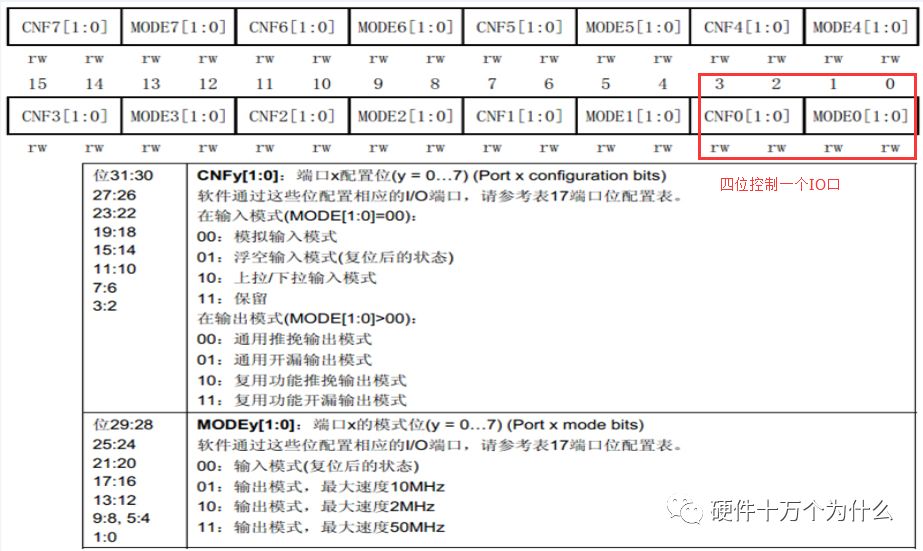
As shown: Taking the low 16 bits of the port configuration register as an example, every four bits control one IO port (the high 16 bits are similar)
MODEx’s 2 bits: Configure IO port output/output mode (1 output type + 3 different output speed modes)
CNFx’s 2 bits: Configure IO port input/output state (controlled by MODEx) input/output mode
Taking GPIOA_CRL as an example, configuring IO port PA0 -> MODE0=00 (input mode) CNF0=10 (pull-up/pull-down input mode). In this configuration, whether it is pull-up or pull-down input mode still needs to be determined by the ODR register.

We will explain the control of pull-up/pull-down in detail below – in the data register – when discussing the ODR output register.
2. Data Register (Taking the Input Data Register GPIOx_IDR as an example)
Each group of IO ports has a 32-bit GPIOx_IDR register (only the low 16 bits are actually used, the high 16 bits are reserved), meaning 16 bits control 16 IO ports, with each bit controlling one

As shown: The IDR register is 32 bits, with bits 0-15 representing the current values of a group of 16 IO ports
Here we have understood the input/output data registers, now let’s discuss the previously mentioned issue:
When the IO port is configured as input mode and set to pull-up/pull-down input mode (i.e., MODEx=00 CNFx=10), the ODR determines whether it is pull-up input (ODRx=0) or pull-down input (ODRx=1)
1) When in output mode, ODR is the output data register
2) When in input mode, ODR is used to distinguish whether the current bit input mode is pull-up input or pull-down input
3. Port Bit Set/Clear Register (GPIOx_BSRR)

The function of the BSRR register:
The BSRR register is a 32-bit register, with the low 16 bits BSx for setting (1 sets, 0 does not change), and the high 16 bits BRx for reset (1: clear, 0: do not change)
Of course, the ultimate goal is still to indirectly set the ODR register through BSRR to change the IO port level
4. Port Bit Clear Register (GPIOx_BRR)

The function of the GPIOx_BRR register is the same as that of the high 16 bits of the GPIOx_BSRR register
Generally, we use the low 16 bits of BSRR and the low 16 bits of BRR (the STM32F4 series has removed the high 16 bits of BSRR)
5. Latch Register: Used less frequently, not analyzed here
7. Port Multiplexing and Remapping
1. Port Multiplexing:
Most IO ports can be multiplexed as external function pins, refer to the chip datasheet (IO port multiplexing and remapping)
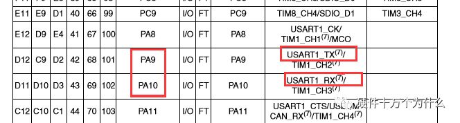
For example: The PA9 and PA10 pins of STM32F103ZET6 can be multiplexed for serial transmission and reception function pins, and can also be multiplexed for Timer 1 Channel 2 and Channel 3
The purpose of port multiplexing: to maximize the utilization of port resources
2. Port Remapping:
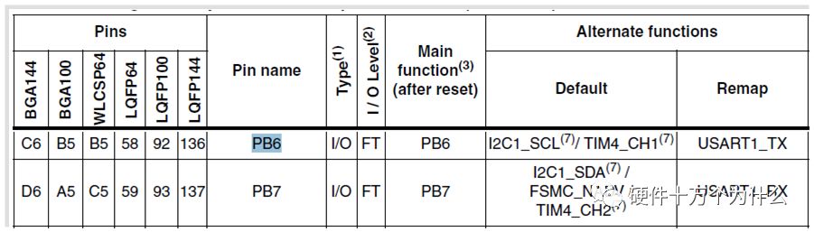
Serial port 1 default pins are PA9, PA10, which can be remapped to PB6, PB7 through configuration
The purpose of port remapping: to facilitate wiring
3. All IO ports of STM32 can be used as interrupt inputs (the 51 microcontroller only has 2 ports that can be used as external interrupt inputs)
3. The Process of GPIO Software Operation
First, we open the LED_DEMO example on the iBox development board (download address is detailed in the previous content: From Schematic PCB to Porting RTOS: A Detailed Discussion on STM32 [Part 2] Create Your Own Project), and click the “Start/stop Debug Session” button at the top of the software, as shown below:

The program starts from the main function. We click the step button in the upper left corner or press the F11 key,
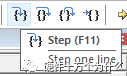
We will find the yellow arrow moves to the main function position:
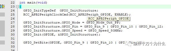
Continuing to press F11, we find the yellow arrow moves to the position shown in the next image:

The above function enables the clock for the GPIOE port. GPIOE belongs to the APB2 high-speed bus, so we use the function RCC_APB2PeriphClockCmd(xxx, xxx) to start the corresponding I/O port. GPIO can only be used when the clock is enabled.
We click again and find that we enter the RCC_APB2PeriphClockCmd (xxx, xxx) function.

assert_param(IS_RCC_APB2_PERIPH(RCC_APB2Periph));
assert_param(IS_FUNCTIONAL_STATE(NewState)); These two lines are used to check whether the parameters are within the specified range. Continuing to press F11, we find the yellow cursor jumps to “RCC->APB2ENR |= RCC_APB2Periph;”. Here, the value of RCC_APB2Periph_GPIOE is assigned to RCC_APB2ENR. We will not go into detail about this function for now.
In the next four single-step runs, we will find the program jumps back to the main function. The yellow arrow will move through the four lines of code shown in the next image.

We analyze line by line:

The first line’s function is to select the working mode of the IO port. Since driving an LED requires a larger current, we use the push-pull output mode here. If we want to change to another mode, we just need to change the “GPIO_Mode_Out_PP” after the equal sign in the above image to another working mode.
GPIO_Mode_Out_PP Push-Pull Output
GPIO_Mode_Out_OD Open-Drain Output
GPIO_Mode_AF_PP Multiplexed Push-Pull Output
GPIO_Mode_AF_OD Multiplexed Open-Drain Output
GPIO_Mode_AIN Analog Input
GPIO_Mode_IN_FLOATING Floating Input
GPIO_Mode_IPD Pull-Down Input
GPIO_Mode_IPU Pull-Up Input

The second line’s function is to select the IO port number. Here we choose GPIOE’s pins 9, 10, and 12. GPIO_Pin_x can have values from 0 to 15; if we want to select multiple IO ports simultaneously, we can use the method shown above with “|” to separate them, or use GPIO_Pin_All to select all ports under the GPIOE group.

The third line’s function is to set the speed of the IO port. The port speed only needs to be set when the IO port is set to output. If it is in input mode, it does not need to be set. The port speed can be 2/10/50MHz. Since we set the IO port working mode to push-pull output, we need to set the IO port speed here.

The fourth line’s function is to run the GPIO initialization library function. It writes the settings from the above three lines into the corresponding registers of the IO port. The first parameter is which group of ports we want to write to. The second parameter is the settings for this group of ports, which is the structure content we just set. This completes the initialization of the three ports.
After executing the next step, we find that the program jumps to the GPIO_Init() function.

This function will be introduced in detail later, so we will not discuss it here.
Directly step out (Ctrl+F11) to the next step. We find that the program returns to the main function at the position shown in the next image.

This uses the function GPIO_SetBits. This function has only two parameters: the first parameter is to select the group of GPIO (here we choose GPIOE); the second parameter is to select the GPIO Pin (here we choose 9, 10, and 12). This function is specifically used to set the IO port (output high level). After executing this function, we can observe that all three indicator lights on the iBox are lit up.
The function corresponding to GPIO_SetBits is GPIO_ResetBits. This function is used to clear the specified data port bits, which is used to set the IO port to zero. The usage is the same as GPIO_SetBits. There are many ways to operate IO ports, which we will gradually introduce later.
Continuing to run the program, we find the yellow arrow jumps to the position shown in the next image:
 GPIOx->BSRR is the port bit set/clear register. Its function is to set or clear the port bits.
Continuing to run, the program jumps back to the main function at the position shown in the next image:

Where “for(; ;)” can be understood as “while(1)”. In comparison, the for-style infinite loop is more efficient.
That is, no initial value is set, no condition is checked, the loop variable does not increment, and there is no termination of the loop; the program will continuously execute the content inside the braces.
The first line inside the braces uses GPIO_SetBits, with the following two parameters being GPIO_LED_PORT and GPIO_LED_ALL. We right-click to select “Go To Definition Of ‘GPIO_LED_PORT'” and it will jump to the position shown in the next image:
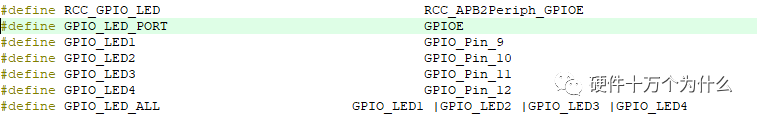
It is not difficult to see that GPIOE is defined as GPIO_LED_PORT; GPIO_Pin_9, GPIO_Pin_10, GPIO_Pin_11, GPIO_Pin_12 are defined as GPIO_LED_ALL.
Thus, we can easily understand the meaning of these four statements: First, using GPIO_SetBits to set the GPIOE group pins 9, 10, 11, and 12 high, after a delay, using GPIO_ResetBits to clear the GPIOE group pins 9, 10, 11, and 12, and after another delay, since this is executed in for(;;), the program will continuously loop here, thus achieving the effect of the LED blinking.
Previous Content:
From Schematic PCB to Porting RTOS: A Detailed Discussion on STM32 [Part 1] Using Official Code to Create a Project
From Schematic PCB to Porting RTOS: A Detailed Discussion on STM32 [Part 2] Create Your Own Project