13.4
Experiment 1: Configuring the System Clock
To briefly explain the idea: using different frequencies for the system clock will result in varying execution times for a simple software delay function in the CPU, leading to different delay effects, which can be judged by the frequency of the LED blinking. The simple software delay function is written by the user and will be provided later.
13.4.1
Hardware Design
This experiment requires the use of an LED. The speed of the LED blinking will help to determine whether the modification of the clock frequency is effective. For explanations of the LED circuit diagrams for the Wildfire Kaiming 6M5, Kaiming 4M2, and Kaiming 2L1 development boards, please refer to the previous section on lighting up the LED, which will not be repeated here.
13.4.2
Software Design
13.4.2.1
Create a New Project
For the e2studio Development Environment
Copy our previous e2s project “11_GPIO_LED”, then rename the project folder to “14_CGC”, and finally import it into our e2studio workspace.
For the Keil Development Environment
Copy our previous Keil project “11_GPIO_LED”, then rename the project folder to “14_CGC”, and double-click the Keil project file inside that folder to open the project.
13.4.2.2
FSP Configuration
Then open the FSP configuration interface for the project. In the clock configuration page, we can modify the MCU main frequency or the clock frequency of other buses. After changing the MCU main frequency, we can also observe the LED blinking frequency to simply judge whether the CPU main frequency has been successfully modified.
Configure the CPU to run at the default frequency of 200MHz
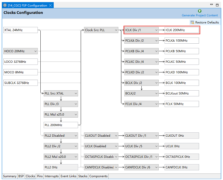
Open the FSP Clock configuration page. The default clock configuration for the RA6M5 is shown in the figure below. The external crystal (XTAL) frequency is set to 24MHz by default, which is consistent with the crystal frequency of the Kaiming 6M5 development board. If it is incorrect, it needs to be modified. Here, we will not make any changes; all configurations will follow the default clock frequency configuration, with the MCU main frequency (ICLK) set to the default of 200MHz.
Click to view the full image
After configuration is complete, click the “GenerateProjectContent” icon in the upper right corner to generate the project content and let the software generate new code content.
In fact, in the bsp_clock_cfg.h file, you can see specific macros related to clock configuration.
Table 2:
Code Listing 14-2 bsp_clock_cfg.h Clock Configuration Related Macros
Swipe left and right to view the full content
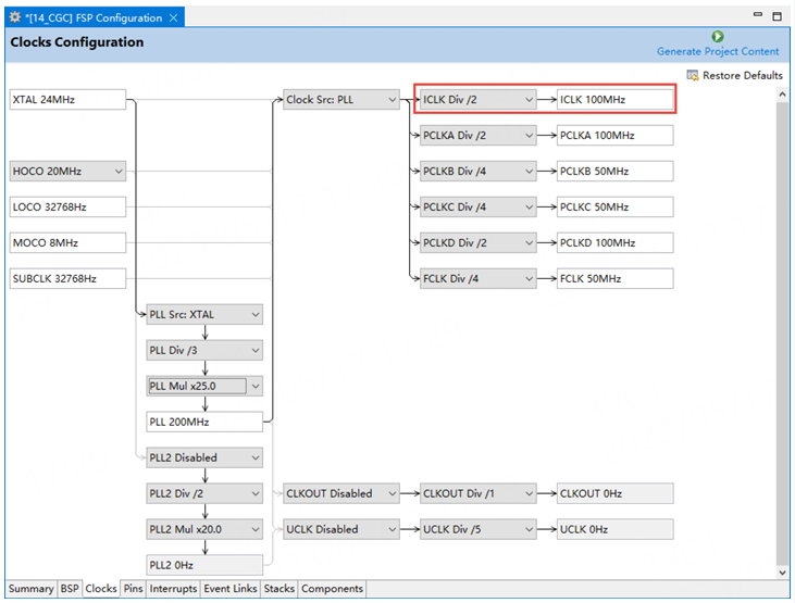
/* generated configuration header file- do not edit */#ifndef BSP_CLOCK_CFG_H_#define BSP_CLOCK_CFG_H_#define BSP_CFG_CLOCKS_SECURE (0)#define BSP_CFG_CLOCKS_OVERRIDE (0)#define BSP_CFG_XTAL_HZ (24000000) /* XTAL 24000000Hz */#define BSP_CFG_HOCO_FREQUENCY (2) /* HOCO 20MHz */#define BSP_CFG_PLL_SOURCE (BSP_CLOCKS_SOURCE_CLOCK_MAIN_OSC) /* PLL Src:␣ →XTAL */#define BSP_CFG_PLL_DIV (BSP_CLOCKS_PLL_DIV_3) /* PLL Div /3 */#define BSP_CFG_PLL_MUL BSP_CLOCKS_PLL_MUL_25_0 /* PLL Mul x25.0 */#define BSP_CFG_PLL2_SOURCE (BSP_CLOCKS_CLOCK_DISABLED) /* PLL2 Disabled */#define BSP_CFG_PLL2_DIV (BSP_CLOCKS_PLL_DIV_2) /* PLL2 Div /2 */#define BSP_CFG_PLL2_MUL BSP_CLOCKS_PLL_MUL_20_0 /* PLL2 Mul x20.0 */#define BSP_CFG_CLOCK_SOURCE (BSP_CLOCKS_SOURCE_CLOCK_PLL) /* Clock Src:␣ →PLL */#define BSP_CFG_CLKOUT_SOURCE (BSP_CLOCKS_CLOCK_DISABLED) /* CLKOUT␣ →Disabled */#define BSP_CFG_UCK_SOURCE (BSP_CLOCKS_CLOCK_DISABLED) /* UCLK Disabled */#define BSP_CFG_OCTA_SOURCE (BSP_CLOCKS_CLOCK_DISABLED) /* OCTASPICLK␣ →Disabled */#define BSP_CFG_CANFDCLK_SOURCE (BSP_CLOCKS_CLOCK_DISABLED) /* CANFDCLK␣ →Disabled */#define BSP_CFG_ICLK_DIV (BSP_CLOCKS_SYS_CLOCK_DIV_1) /* ICLK Div /1 */#define BSP_CFG_PCLKA_DIV (BSP_CLOCKS_SYS_CLOCK_DIV_2) /* PCLKA Div /2 */#define BSP_CFG_PCLKB_DIV (BSP_CLOCKS_SYS_CLOCK_DIV_4) /* PCLKB Div /4 */#define BSP_CFG_PCLKC_DIV (BSP_CLOCKS_SYS_CLOCK_DIV_4) /* PCLKC Div /4 */#define BSP_CFG_PCLKD_DIV (BSP_CLOCKS_SYS_CLOCK_DIV_2) /* PCLKD Div /2 */#define BSP_CFG_BCLK_DIV (BSP_CLOCKS_SYS_CLOCK_DIV_2) /* BCLK Div /2 */#define BSP_CFG_BCLK_OUTPUT (2) /* BCLK/2 */ #define BSP_CFG_FCLK_DIV (BSP_CLOCKS_SYS_CLOCK_DIV_4) /* FCLK Div /4 */#define BSP_CFG_CLKOUT_DIV (BSP_CLOCKS_SYS_CLOCK_DIV_1) /* CLKOUT Div /1 */#define BSP_CFG_UCK_DIV (BSP_CLOCKS_USB_CLOCK_DIV_5) /* UCLK Div /5 */#define BSP_CFG_OCTA_DIV (BSP_CLOCKS_OCTA_CLOCK_DIV_1) /* OCTASPICLK Div / →1 */#define BSP_CFG_CANFDCLK_DIV (BSP_CLOCKS_CANFD_CLOCK_DIV_6) /* CANFDCLK␣ →Div /6 */#endif/* BSP_CLOCK_CFG_H_ */The clock configuration page for the RA4M2 is shown in the figure below:
Click to view the full image
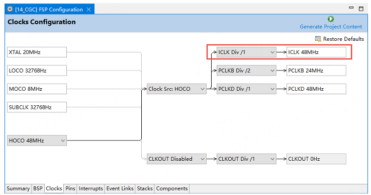
The clock configuration page for the RA2L1 is shown in the figure below:
Click to view the full image
Note
The XTAL external crystal frequency in the RA2L1 clock configuration shown above is inconsistent with the crystal frequency (8MHz) on the Kaiming 2L1 development board. Therefore, if the user needs to use an external crystal to provide clock input, the “XTAL20MHz” in the figure needs to be changed to “XTAL 8MHz”.
First, let us test the LED blinking effect at a main frequency of 200MHz using a simple software delay function. Readers are encouraged to jump to the section on the “hal_entry entry function” to continue reading.
Configure the CPU to run at a frequency of 100MHz
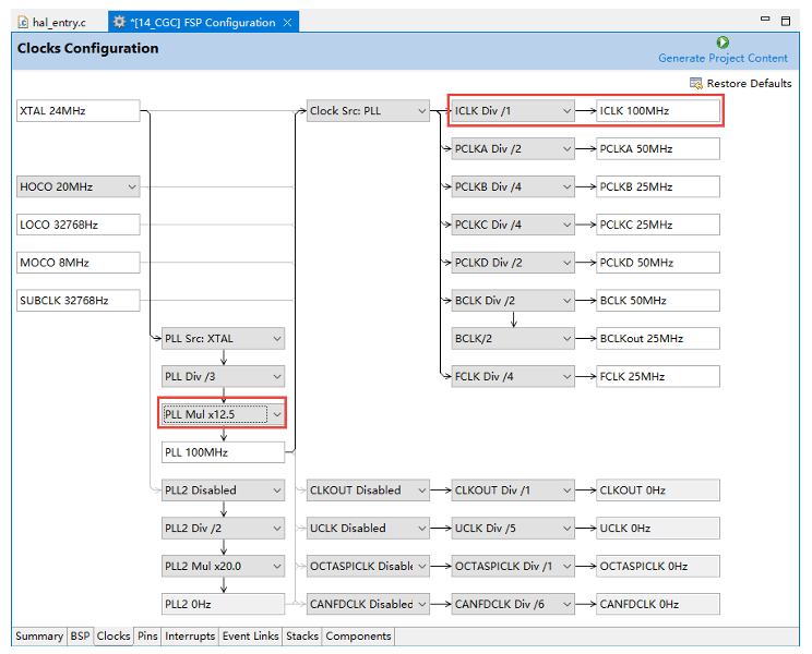
Open the Clock configuration page for the RA6M5, as shown in the figure below, and change PLLMul to x12.5, which changes the PLL multiplication factor from the original 25 times to 12.5 times. The main frequency then becomes 100MHz.
Click to view the full image
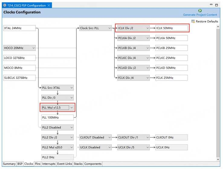
Open the Clock configuration page for the RA4M2 and modify it as shown in the figure below.
Click to view the full image
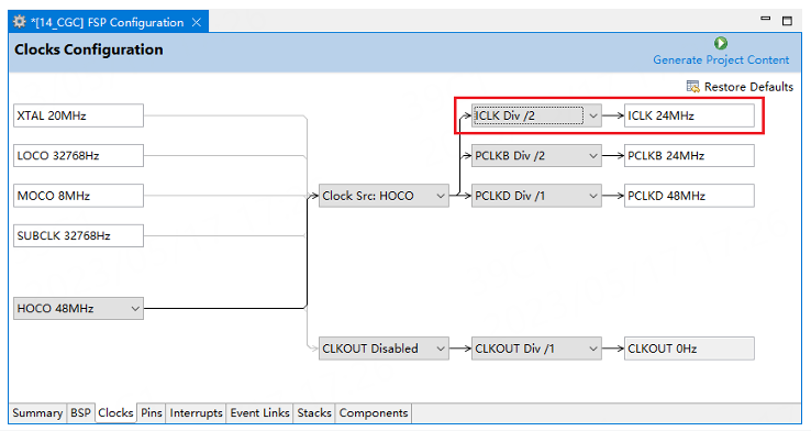
Open the Clock configuration page for the RA2L1 and modify it as shown in the figure below.
Click to view the full image


Need Technical Support?
If you have any questions while using Renesas MCU/MPU products, you can scan the QR code below or copy the URL into your browser to access the Renesas Technical Forum to find answers or get online technical support.

https://community-ja.renesas.com/zh/forums-groups/mcu-mpu/
To be continued
Recommended Reading
CGC Clock Configuration Block Diagram Analysis – Renesas RA Series FSP Library Development Practical Guide (30)

Clock Source – Renesas RA Series FSP Library Development Practical Guide (31)
PLL2 Phase-Locked Loop – Renesas RA Series FSP Library Development Practical Guide (32)