Abstract
Introduction
1. Bootloader and Application Program Memory Address Allocation for MPC5744P
1.1 SRAM Resources of MPC574xP Series MCU
1.2 Flash Resources of MPC574xP Series MCU
1.3 CAN Bus Bootloader and Application Program Memory Address Allocation for MPC5744P
2. Flash Driver Development (Installation, Downloading, and Using C55 Flash SSD)
3. FlexCAN Driver Development
3.1 DEVKIT-MPC5744P CAN Bus Hardware Design
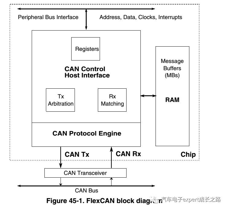
3.2 Introduction to FlexCAN Module Features of Qorivva MPC57xx Series MCU
Qorivva MPC57xx series MCUs use the FlexCAN module for CAN bus communication, which has the following features:
3.3 FlexCAN Module Communication Baud Rate Configuration
3.4 FlexCAN Module RX ID Filter Settings, Interrupt Settings, and Driver API Introduction
4. Introduction to Upper Computer Software and CAN Bus Communication Protocol
5. Introduction to Bootloader Program Flow (Parsing S19 Files, Calling Flash SSD Programming Applications, and Jump Methods)
6. Using the Bootloader Introduced in This Article
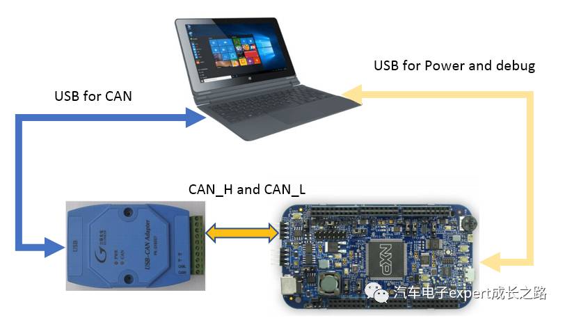
6.1 Test Hardware Connection Based on DEVKIT-MPC5744P
6.2 Testing This Bootloader on DEVKIT-MPC5744P
Conclusion
Introduction
The Qorivva MPC57xx series automotive-grade MCUs have been in mass production since the end of 2015 and are widely used in various automotive electronic ECU products. In automotive electronic ECUs, there is an increasing demand for developing bootloader functionality based on CAN bus communication to enable online application upgrades or to interface with future vehicle networking-based FOTA (Firmware Over-The-Air) capabilities.
Compared to previous S12(X) series MCUs, the Qorivva MPC57xx series automotive-grade MCUs have more complex peripheral functional modules, larger and more complex on-chip integrated memory (SRAM and Flash modules). Additionally, their software development environment, S32DS for Power V1.0/1/2, is relatively new, having been released for less than two years, and users are not very familiar with it. These factors make the bootloader for the Qorivva MPC57xx series automotive-grade MCUs somewhat challenging.
Considering the above, the author has developed the CAN bus bootloader for the MPC5744P based on the C55 Flash SSD and S32DS for Power V1.2, and it has been tested successfully on the DEVKIT-MPC5744P.
This article aims to introduce the bootloader development process and considerations for the MPC57xx series MCUs using the MPC574xP as an example, hoping to be helpful to everyone.
Tips: For general principles and considerations regarding automotive electronic ECU bootloader development, please refer to the previous article of this public account titled “Detailed Points of Automotive Electronic ECU Bootloader Development” (click to read directly);
1. Bootloader and Application Program Memory Address Allocation for MPC5744P
1.1 SRAM Resources of MPC574xP Series MCU
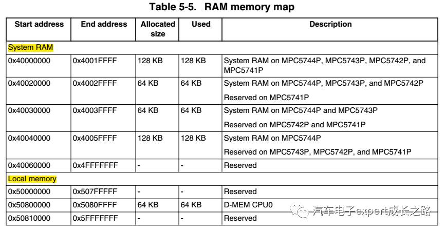
The SRAM of the MPC574xP series MCU includes System RAM and Local Memory. The address mapping allocation in the CPU core addressing space is as follows:
System RAM: Address 0x4000_0000 ~ 0x4005_FFFF, up to 384KB, different part numbers have different sizes;
Local Memory: Address 0x5080_0000 ~ 0x5080_FFFF, all part numbers are 64KB;
Tips:
A. The size of System RAM varies among different part numbers in the same series of MCUs. The specific SRAM address mapping for the MPC574xP series MCUs is as follows:
B. Accessing local memory is more efficient than accessing system RAM, and in multi-core MCUs, each core’s local memory can only be accessed by itself. Therefore, the stack allocation for application projects running on that core is generally assigned to its local memory, which not only improves the core’s execution efficiency but also avoids access conflicts for shared memory resources among multiple cores. Of course, it can also be allocated for other data segments of the application project, such as .data or .bss segments;
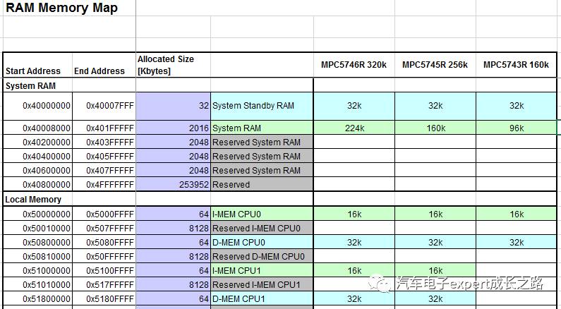
Below is the SRAM address mapping for multi-core MCUs–MPC574xR series, where the local memory addresses for multi-core CPUs are independently separated:
1.2 Flash Resources of MPC574xP Series MCU
The on-chip Flash of the MPC57xP series MCU includes 16KB UTest Flash, 96KB Data Flash, and up to 2464KB Code Flash, as well as corresponding Mirror Flash:
UTest Flash: Address 0x0040_0000 ~ 0x0040_3FFF, total 16KB, system reserved area, user stores Flash and chip configuration information, such as UDF records, ADC trim parameters, and IRC trim values;
Data Flash: Address 0x0080_0000 ~ 0x0081_7FFF, total 96KB, 4 blocks, occupying 3 RWW partitions, generally used as emulated EEPROM; of course, it can also be used to store user application code and data when not used as emulated EEPROM;
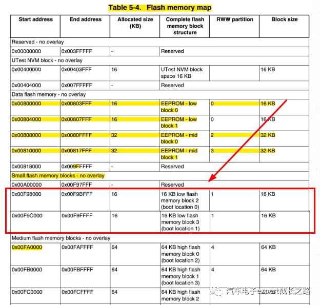
Code Flash: Includes 416KB of Small and Medium Flash blocks, Address 0x00A0_0000 ~ 0x00A5_FFFF, and up to 2MB of Large Flash blocks, Address 0x0100_0000 ~ 0x011F_FFFF, which are primarily used to store user application code and data, but can also be used for emulated EEPROM if needed.
Mirror Flash: This area consists of 384KB of Small and Medium Code Flash mirror Flash from address 0x08A0_0000 ~ 0x08A5_FFFF and up to 2MB of Large Flash mirror Flash blocks from address 0x9100_0000 ~ 0x911F_FFFF. This is a system reserved area and is not programmable by the user;
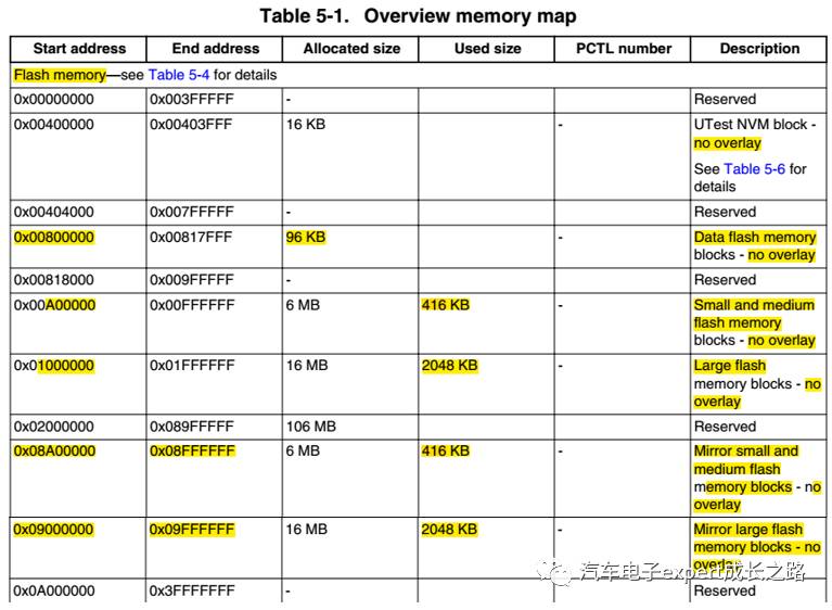
MPC5744P has a total of 2.5MB of on-chip Flash memory, including 4 16KB Low Flash Blocks (4*16KB = 64KB), 2 32KB Mid Flash Blocks (2*32KB = 64KB), 6 64KB High Flash Blocks (6*64KB = 384KB), and 8 256KB Flash Blocks (8*256KB = 2MB):
64KB + 64KB + 384KB + 2MB = 2.5MB
The specific mapping addresses and Flash Block allocation for MPC5744P, as well as RWW partition and Block sizes, are shown in the following table:
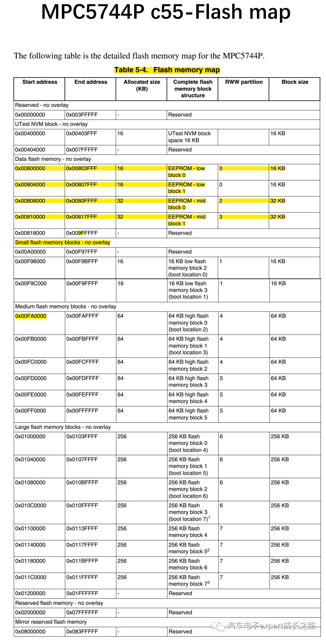
Flash Blocks belonging to different RWW partitions support Read-While-Read operations, allowing the Flash driver of Block A to operate on Block B; the 96KB Flash space from address 0x80000~0x817FFF includes Low Flash Blocks 0~1 and Mid Flash Blocks 0~1, totaling 4 Flash Blocks allocated for emulated EEPROM. In the entire 2.5MB Flash address space, only Low Flash Blocks 2~3, High Flash Blocks 0~1, and 256KB Flash Blocks 0~3 can serve as boot locations (boot location 0~7).
The so-called boot location is the area where the legitimate boot half-word and reset vector are searched when the MCU is reset. After reset, the CPU will sequentially look for a legitimate reset configuration half-word (RCHW) composed of the boot_ID–0x5A from boot location 0~7 (the high 16-bit is RCHW, the low 16-bit is reserved, located at the starting address of the Flash block) and the application start address (32-bit reset vector, located at the starting address of the Flash block offset by 0x4):
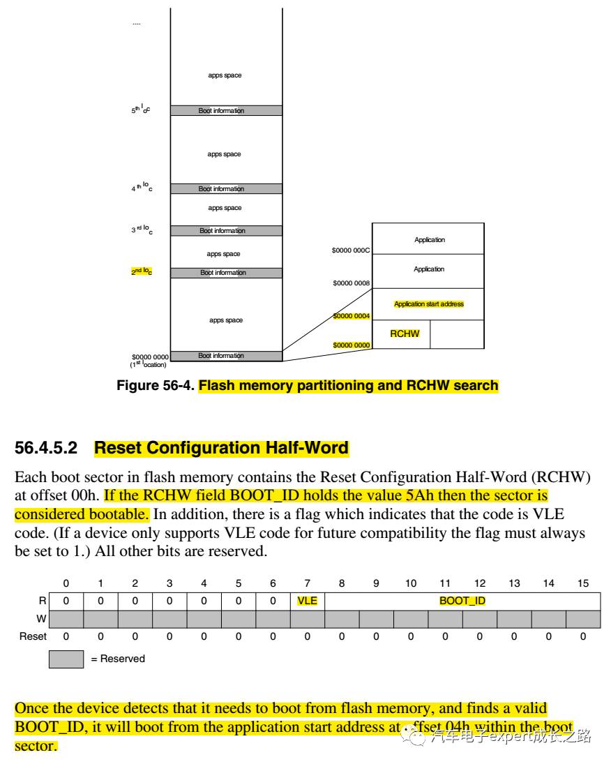
Tips: The PowerPC e200zx series CPU core is different from other MCU cores like S08, S12(X), and ARM Cortex-M cores, as the address where the application program starts after reset (commonly referred to as the reset vector) is not placed in the interrupt or exception vector table but is kept at the Flash Block address offset by 0x4 of the boot location. Therefore, when developing the bootloader for the Qorivva MPC57xx series MCUs based on the PowerPC e200zx core, to ensure that the bootloader runs first after each power-up, the bootloader’s startup function address and the correct boot_ID must be placed in a boot location Flash Block that is earlier/smaller than the application startup function address and correct boot_ID residing Flash Block.
Tips: For an introduction to the Flash module functions of the MPC57xx series MCUs, please refer to the previous article of this public account titled “Detailed Explanation of the C55 Flash Module and Its SSD (Standard Software Driver) Usage of the MPC57xx Series MCUs” (click to read directly);
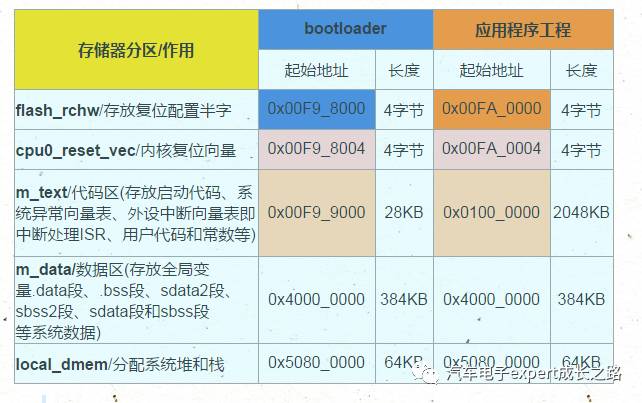
1.3 CAN Bus Bootloader and Application Program Memory Address Allocation for MPC5744P
In light of the above, the bootloader design introduced in this article will allocate the two 16KB Small Flash Blocks where boot location 0 and 1 reside as storage space for the bootloader, and the bootloader’s startup configuration half-word and startup function address will be specified at the initial address 0x00F9_8000 ~ 0x00F9_8007.
This is specifically achieved by modifying the project’s linker file:
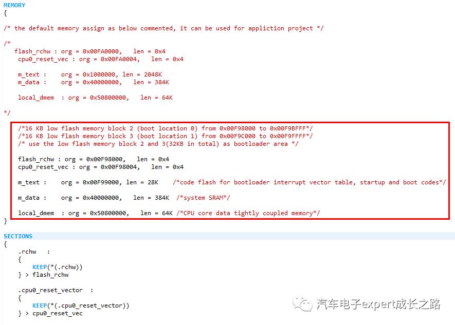
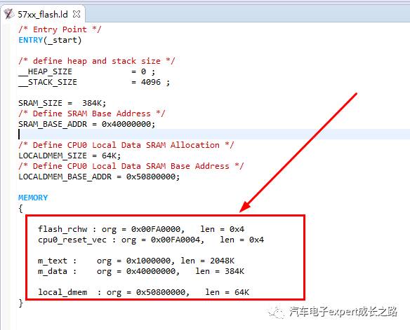
The default linker file for a new application project in S3DS for Power v1.2 is as follows, which allocates the above Flash Blocks and uses 4 Flash Blocks (total 96KB) as emulated EEPROM:
Therefore, the memory address allocation for the bootloader project and the application project introduced in this article is shown in the following table:
2. Flash Driver Development (Installation, Downloading, and Using C55 Flash SSD)
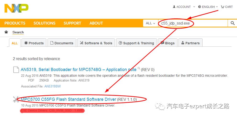
The bootloader introduced in this article uses the MPC57xx C55FG Flash SSD (REV 1.1.0) provided by NXP’s official website. You can download it by entering “c55_jdp_ssd.exe” in the search bar of NXP’s official website www.nxp.com:
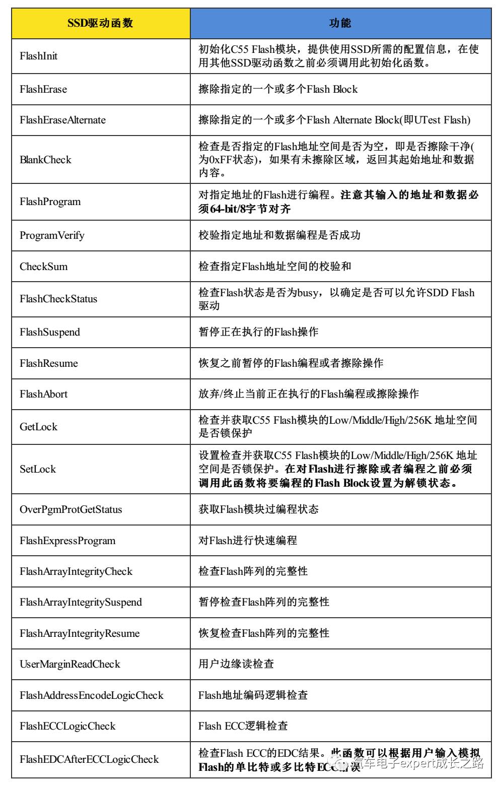
This SSD provides the following Flash driver functions, with their corresponding functionalities shown in the table:
Tips:
A. For the usage of the C55 Flash module and its SSD driver in the MPC57xx series MCUs, please refer to the previous article of this public account titled “Detailed Explanation of the C55 Flash Module and Its SSD (Standard Software Driver) Usage” (click to read directly), which will not be elaborated here.
B. Based on the introduction in section 1.3–CAN Bus Bootloader and Application Program Memory Address Allocation for MPC5744P, this example uses the 32KB Flash of RWW partition 1 (the only 32KB address space in RWW partition) as the bootloader storage space, while the remaining Flash address space allocated for the application program belongs to different RWW partitions. Therefore, the SSD can be stored in the bootloader’s Flash space and directly run Flash driver functions to erase and program the application program Flash space.
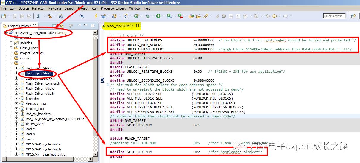
In the SSD configuration fileblock_mpc574xP.h, defineUNLOCK_LOW_BLOCKS as 0x0000000C to lock the protective eyes allocated to the bootloader project for low Flash blocks 2 and 3, while the remaining Flash blocks (UNLOCK_MID_BLOCKS and UNLOCK_HIGH_BLOCKS) are set to 0–unlock protection to prevent accidental erasure, and set SKIP_IDX_NUM to 0x2 (2 blocks):
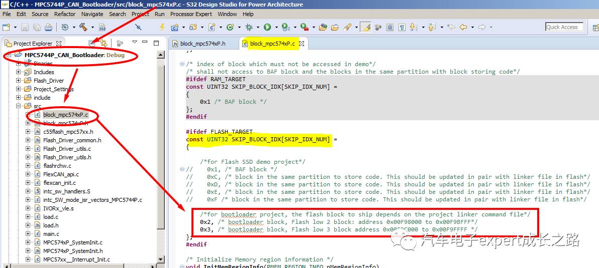
And define the array member of UINT32 SKIP_BLOCK_IDX[SKIP_IDX_NUM] in block_mpc574xp.c as 0x2 and 0x3, so that it can complete unlocking protection and erasing all Flash blocks allocated to the application program outside of the bootloader:
C. If you want to develop a dual boot mode bootloader that can also update itself, and want to run the Flash SSD in SRAM, you can refer to the previous article of this public account titled “S32DS Usage Tips–Detailed Explanation of Linker Files and Startup Process for S32DS for Power V1.2” (click to read directly) for the method and steps to automatically copy the redirection function in the custom code segment to RAM.
3. FlexCAN Driver Development
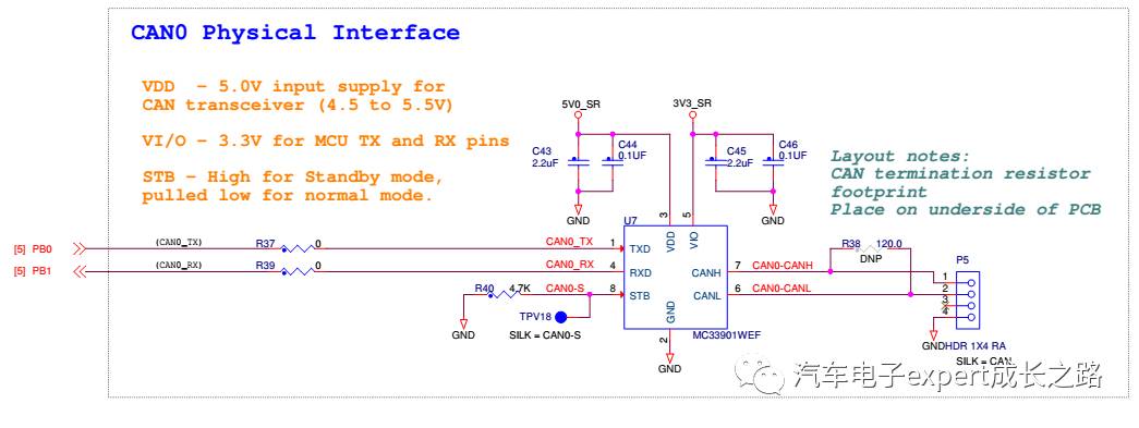
3.1 DEVKIT-MPC5744P CAN Bus Hardware Design
In this design, the FlexCAN0 of DEVKIT-MPC5744P is used to communicate with the upper computer software to obtain the application program, which is connected to the onboard CAN transceiver MC33901 (enabled by default) and is drawn from P5.
3.2 Introduction to FlexCAN Module Features of Qorivva MPC57xx Series MCU
Qorivva MPC57xx series MCUs use the FlexCAN module for CAN bus communication, which has the following features:
-
Full implementation of BOSCH’s CAN bus protocol specification CAN 2.0B
-
Supports standard data frames and remote frames;
-
Supports extended data frames and remote frames;
-
0~8 bytes of data length;
-
Programmable communication baud rate, up to 1Mbps;
-
Content-related addressing
-
Compatible with ISO11898-1 standard;
-
0~8 bytes of flexible message mailbox (MB-MailBox);
-
Each message mailbox (MB) can be configured for sending or receiving, and supports both standard frame and extended frame messages;
-
Each message mailbox (MB) has its own independent RX mask register for ID filtering;
-
Full RX FIFO storage capability, supporting up to 6 frames of data reception and automatic internal pointer processing;
-
Supports transmission termination function;
-
Programmable clock source selection, can choose bus clock or external crystal clock;
-
Unused buffer RAM space can be used as general RAM space;
-
Compatible with listen mode;
-
Programmable brilliant mode to support self-test operations;
-
Programmable transmission priority scheduling strategy: minimum ID first, minimum buffer first, or highest buffer first;
-
16-bit only runtime timestamp;
-
Global network time synchronization for specific messages;
-
Interrupts can be masked;
-
Transmission medium independence (external transceiver);
-
High priority message arbitration will have short delay times;
-
Supports low power mode;
-
Also provides some important new features:
-
Remote request frames can be processed automatically or with software;
-
CAN bit time settings and configuration bits can only be written in module freeze mode;
-
TX message mailbox (MB) status;
-
Receiving message frame ID filter hit prompt (IDHIT);
-
The SYNCH bit in status register 1 indicates that the module is synchronized with the CAN bus;
-
CRC status of sent messages;
-
Receiving FIFO global mask register;
-
In matching processing, message mailbox priority and receiving FIFO can be selected;
-
Provides powerful receiving FIFO ID filter, which can be set to filter 128 extended frames, 256 standard frames, or 512 partial (8-bit) IDs, as well as 32 independent IDs;
-
100% forward compatibility with older FlexCAN modules;
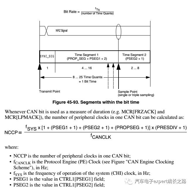
3.3 FlexCAN Module Communication Baud Rate Configuration
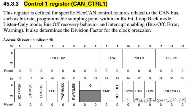
In this bootloader development, the FlexCAN of MPC5744P is configured to use an external 40MHz crystal oscillator as the clock source, by configuring the FlexCAN module’s control register 1 (CAN_CTRL1) to achieve a communication rate of 500Kbps:
CAN_0.CTRL1.R = 0x0414C036;
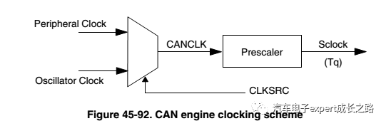
The baud rate calculation formula for the FlexCAN module is as follows:
3.4 FlexCAN Module RX ID Filter Settings, Interrupt Settings, and Driver API Introduction
By calling the API function:
CAN0_ReceiveInit(MB6, StandardFrame, DataFrame, 0x64,0xFFF);
/*receive only standard ID 0x64 for bootloader download CAN frame ID*/
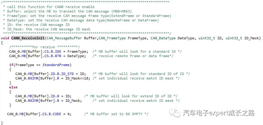
Configure the independent mask register (CAN_RXIMRn) and the receiving message mailbox (MB) to set mailboxMB6 to only receiveID=0x64 standard data frame, which is the CAN message frame ID for downloading data from the upper computer software in this bootloader design;
Configure interrupt mask register 1 (CAN_IMASK1) to enableMB6 receiving interrupt:
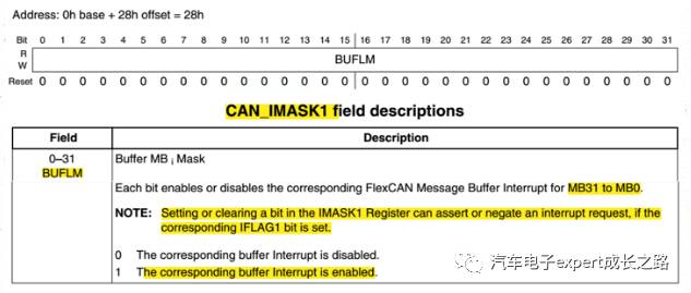
CAN_0.IFLAG1.R = 0x000000F0;/*clean the flags first*/
CAN_0.IMASK1.R = 0x000000F0;
Tips: The sending completion and receiving data ready interrupts for each MB of the FlexCAN module are controlled by a corresponding bit in CAN_IMASK1/2, so to avoid generating interrupts for MB used in polling mode after sending data, the corresponding MB interrupt enable bits need to be cleared;
And configure the interrupt priority registerINTC_0.PSR[523] to set its interrupt priority to 3:
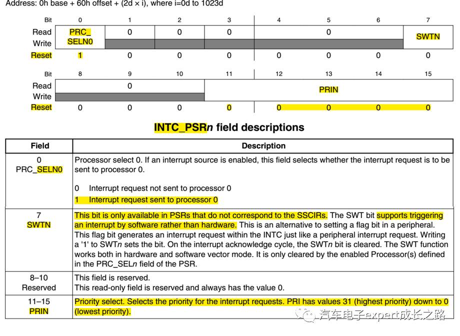
INTC_0.PSR[523].R = 0x8003;/*priority of FlexCAN0 BUF47 as 3*/
In the interrupt ISR of MB4~7 (which share the same interrupt vector and ISR), call the API:
CAN_RxMsg = CAN0_ReceiveMsg(MB6);/*copy the received CAN data into RAM*/
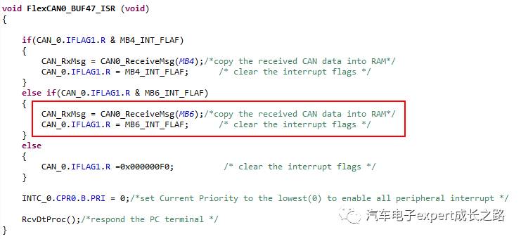
Receive the CAN message frame received by MB6.
Call the API:CAN0_TransmitMsg(MB0,CAN_TxMsg);
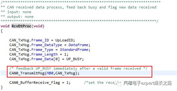
Use polling mode withMB0 to send the CAN message frame in response to the upper computer software.
Tips: Setting the FlexCAN’s receiving ID filter to only receive the ID used for downloading data from the upper computer software can avoid CPU interruptions from unrelated CAN messages, thereby improving the bootloader efficiency.
4. Introduction to Upper Computer Software and CAN Bus Communication Protocol
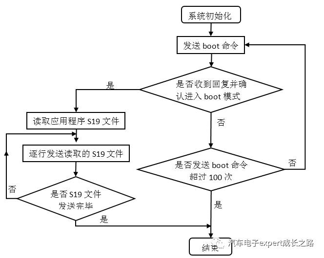
The upper computer software running on the PC mainly reads the application program S19 file of the target MCU and uses a USB to CAN bus adapter to download it line by line to the target MCU. The software design flowchart is as follows:
In this design, Visual C++ is used to call WFC and the GY8507 USB to CAN adapter driver from Wuhan Jiyang Optoelectronics to write the upper computer interface software.
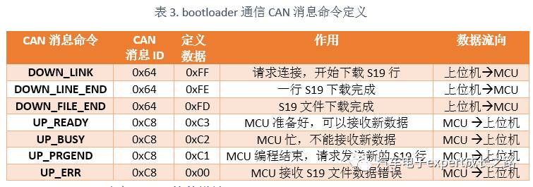
The CAN message for the PC upper computer to download the application S19 file has an ID of 0x64, while the CAN message frame that the bootloader host program responds to the upper computer has an ID of 0xC8, with a communication rate set to 500Kbit/s. Therefore, during S12G initialization, the receiving ID filter of the MSCAN module is set to only receive standard frames with ID 0x64 to avoid interference from other ECUs on the normal network. The specific CAN message command definitions are as follows:
5. Introduction to Bootloader Program Flow (Parsing S19 Files, Calling Flash SSD Programming Applications, and Jump Methods)
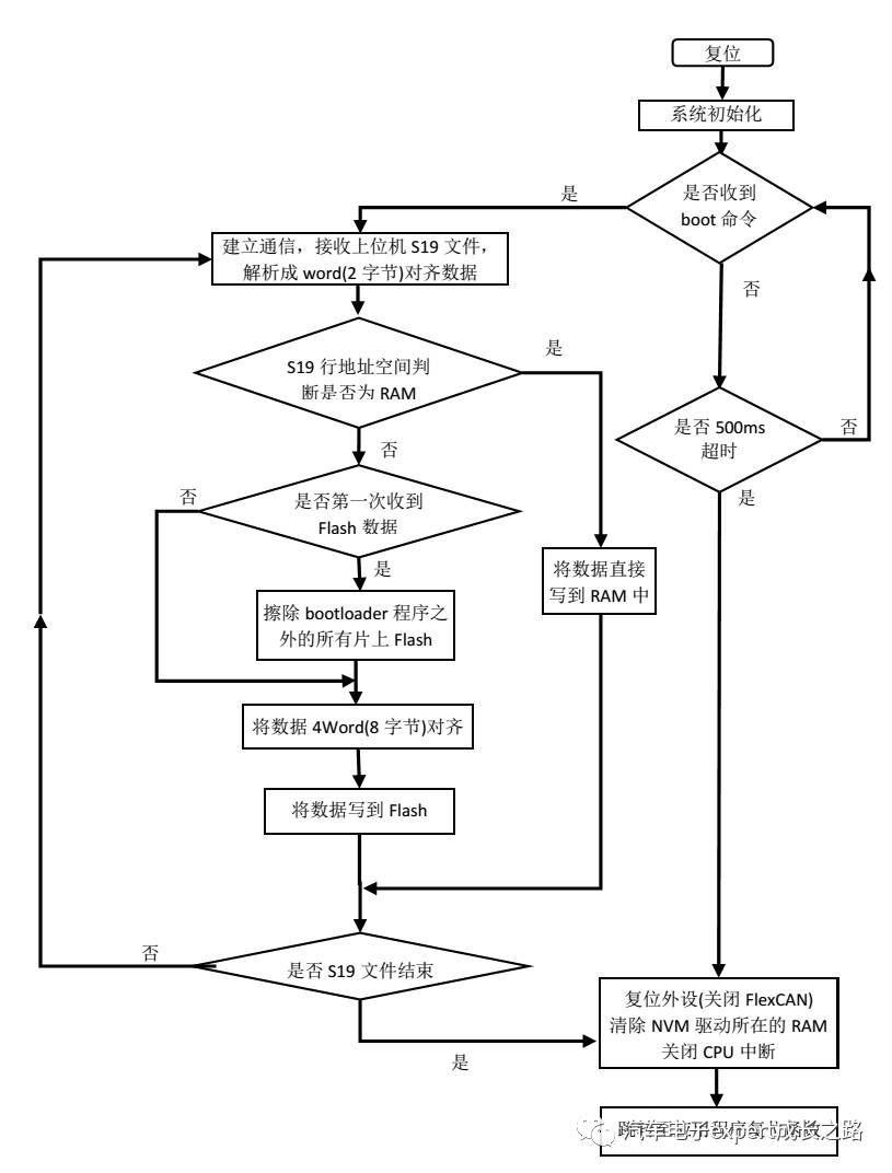
After each MCU reset (including power-on reset, watchdog reset, external input reset, low voltage detection reset, clock detection reset, and illegal address reset), system initialization is performed, system clock is configured, timers are turned on, FlexCAN is configured, and GPIO for state indication is controlled, then the CPU global interrupt is turned on, and it waits for the upper computer boot command and checks for timeout:
If the upper computer request to enter boot mode is received within the specified 500ms, data is received and parsed to obtain the line address and word-aligned data (1 word = 2 Bytes), then the S19 line address space is determined;
If it is a Flash address and it is the first time receiving Flash data, all on-chip Flash except for the bootloader program will be erased to prepare for programming the application program; for data at Flash addresses, the parsed results’ addresses and data must be aligned to 4 words (8 bytes) before programming into Flash to meet the ECC requirements of the MPC57xx series MCU C55 Flash;
If it is a RAM address, no erasure is needed, and the data will be directly written to the specified RAM address;
Then establish communication with the upper computer, receive line by line, parse, and write the results into the corresponding address in on-chip Flash/EEPROM/RAM until the entire application S19 file ends, and finally reset the peripherals (turn off MSCAN), clear all system RAM space, turn off CPU global interrupts, disable all peripheral interrupts, end the bootloader, and jump to the application reset function to execute the application program;
If the upper computer’s boot command sent via CAN is not received within the specified 500ms, the CPU global interrupts are directly turned off, all external interrupts are disabled, the bootloader ends, and jumps to the application reset function to execute the application program.
The software flowchart for the entire bootloader project is as follows:
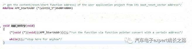
According to the introduction in section 1.3, based on the startup process of the Power e200 core, the startup function address of the application project is stored at address 0x00FA_0004, so it only needs to be retrieved and converted to a function pointer to jump to the application.
Tips: Before the bootloader jumps to the application, it is advisable to restore the peripherals used in the bootloader to their initial state/configuration and clear all RAM to ensure that the running environment when jumping from the bootloader to the application is as consistent as possible with running the application independently, to avoid impacts caused by the bootloader.
The newly created application project in S32DS for Power v1.2 will not generate an S19 file after compilation and linking; it is necessary to configure the project properties to enable Create flash image:
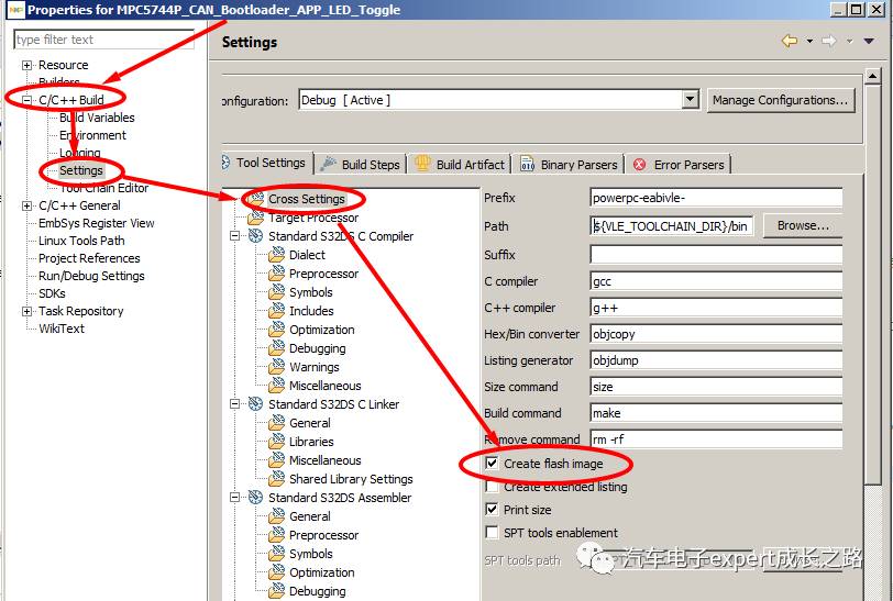
Select Motorola S-record:
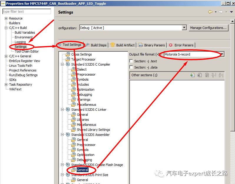
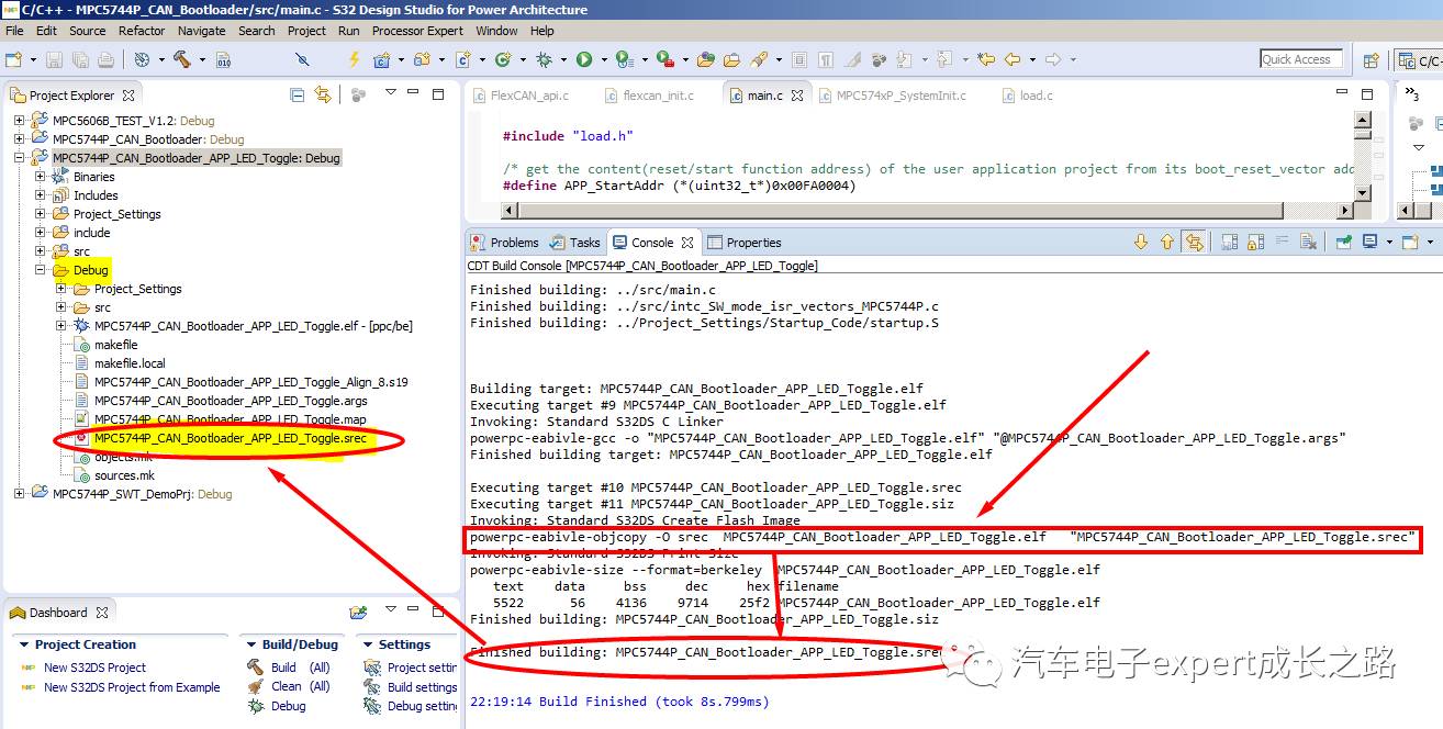
After this configuration, recompiling the application project will generate an S19 file with the same name as the project in the FLASH subdirectory, with a default extension of .srec, which needs to be manually changed to .s19:
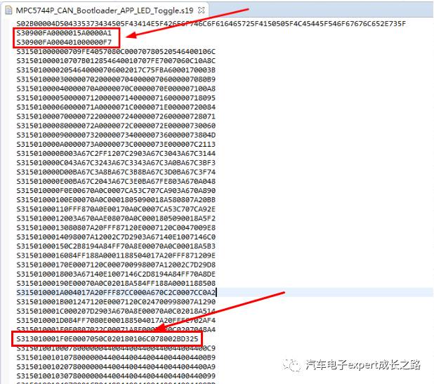
In the automatically generated S19 file of S32DS for Power v1.2, there are cases of non-8-byte address alignment:
Therefore, it is necessary to use other software (such as hexviewer) to align it to 8 bytes before downloading:
For example, in the S19 file compiled for this application project, the length of Block 1 is 0x1FE=510 bytes, while the length of Block 2 is 0xF4=244 bytes, which are not 8-byte aligned:
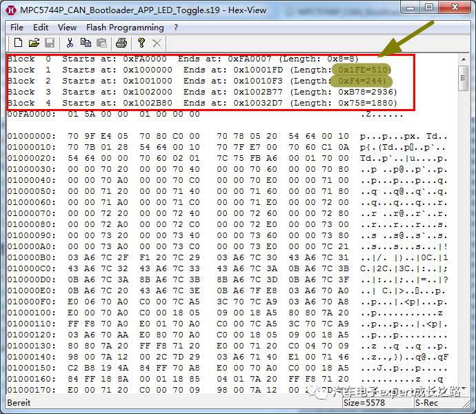
Open it with Hexviewer, and then go to the menu Edit-->Data Alignment, to open the alignment configuration window
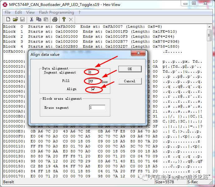
In the alignment settings window, set Segment alignment to 8, Fill (fill) 0xFF, and enable Align:
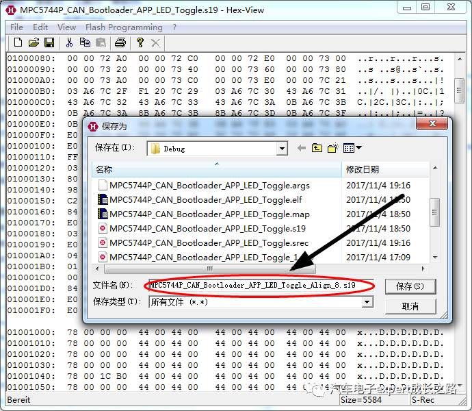
Save it as another name:
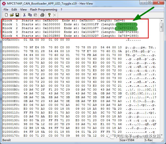
The aligned result is as follows, where both Block 1 and Block 2 are aligned to 8 bytes.

6. Using the Bootloader Introduced in This Article
6.1 Test Hardware Connection Based on DEVKIT-MPC5744P
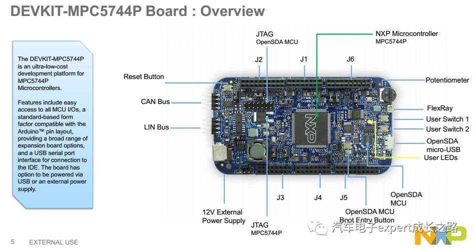
This example is developed and tested based on DEVKIT-MPC5744P and the GY8507 USB-CAN Adapter from Jiyang Optoelectronics. The corresponding hardware connection is shown in the following figure:
6.2 Testing This Bootloader on DEVKIT-MPC5744P
After connecting the computer and hardware as shown above,
First, download the Baidu Cloud share provided at the end of this article, and import the bootloader and test application project contained in MPC5744P_CAN_Bootloader_and_APP_two_in_one_package_DEKIT-MPC5744P_test_OK_2017.11.09.zip into S32DS for Power V1.2 (through the menu File–>Import..–>General–>Existing projects into workspace),
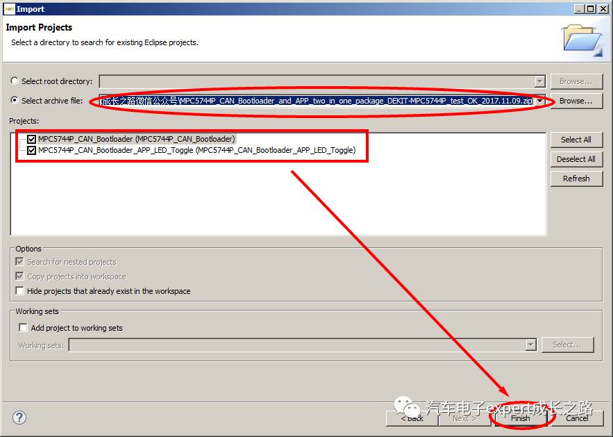
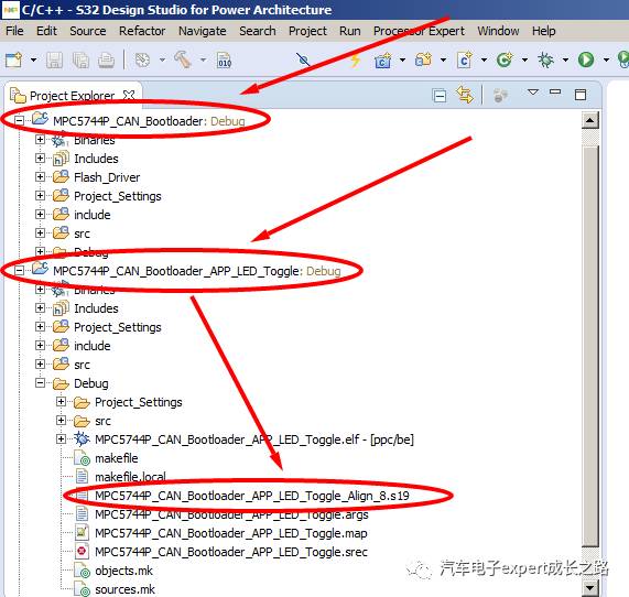
and download the MPC5744P_CAN_Bootloader project into the DEVKIT-MPC5744P via the onboard OpenSAD debugger;
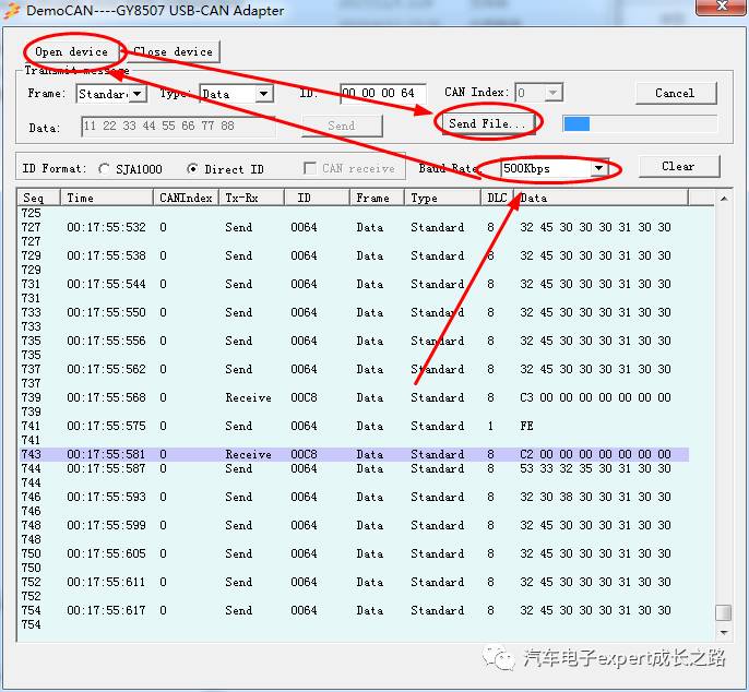
Then, open the upper computer software developed based on the GY8507 USB-CAN Adapter to download the S19 file of the test application:
Step 1: Select the communication baud rate–500Kbps;
Step 2: Click “Open driver” to open the GY8507 USB-CAN Adapter;
Step 3: Click “Send File…” to select the already 8-byte aligned test application–MPC5744P_CAN_Bootloader_APP_LED_Toggle‘s S19 file–MPC5744P_CAN_Bootloader_APP_LED_Toggle_Align_8.s19, and start sending/downloading;
Finally, reset (press the external reset button SW3 or power on reset POR) the DEVKIT-MPC5744P, and the update of the test application will begin:
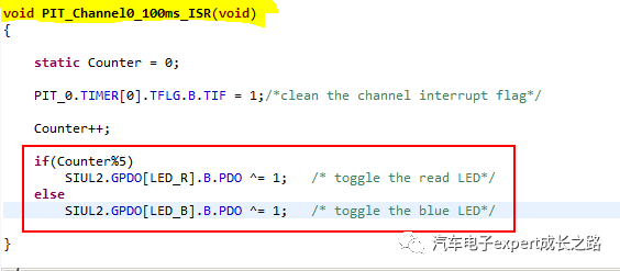
After the update is complete, the MCU will automatically jump to the test application, and the onboard RGB LED light will be toggled by the PIT interrupt, with the red and blue LEDs flashing alternately.
Tips: During the downloading process, a pause screen may appear initially. This is because the bootloader is erasing the on-chip Flash of the MPC5744P, which takes a longer time, during which the upper computer pauses downloading data, waiting for the erasure to complete.
Conclusion
This article comprehensively introduces the development of the CAN bus bootloader for the MPC5744P and elaborates on the challenges in Flash driver, FlexCAN configuration, memory address space division, and bootloader to application program jump, providing methods and steps for testing and verification on the DEVKIT-MPC5744P demo board.
Although this is a bootloader development example for the MPC5744P series MCU, it also has reference significance for the bootloader development of other MPC57xx series MCUs.
I have shared the bootloader project, test APP application project, and matching upper computer software introduced in this article on Baidu Cloud, which everyone can download for reference and study. I hope it is helpful to everyone.
Link: https://pan.baidu.com/s/1slDOwET;
Password: xbtf
This concludes the content I shared with everyone today. I hope it is useful to you.
Original writing is not easy. If you find this article helpful for your work and study, I also welcome everyone to reward and encourage me—- I will continue to write and bring more wonderful original articles to everyone.
Tips: Readers using Android phones can directly click the reward link at the end of the article to reward; readers using iPhones can no longer use WeChat reward functions due to Apple Inc. closing this feature, please use WeChat to scan the QR code below to reward and encourage the author.
Thank you!


This public account has published personal original quality—- links to embedded system technology articles as follows, welcome everyone to refer to and share:
-
Series of Articles on the Growth Path of Automotive Electronics Expert Public Account
-
Detailed Points of Automotive Electronic ECU Bootloader Development
-
Independent NVM Driver Safe Bootloader Development Based on CAN Bus Communication for S12(X) Series MCU
-
Discussion on Three Common Misunderstandings in Embedded MCU Development
-
Discussion on Stack and Heap in Embedded MCU Software Development
-
Discussion on Interrupt Priority and Interrupt Nesting in Embedded MCU Software Development
-
Discussion on Code Style and Code Optimization in Embedded MCU Software Development
-
Detailed Explanation of the Startup Process in Embedded MCU Software Development (From Reset Vector to Preparation Before Main Function)
-
Detailed Explanation of Startup Process in Embedded MCU Software Development (Implementing Custom RAM Initialization in CodeWarrior 5.1)
-
Three Ways to Write Interrupt ISR in CodeWarrior 5.1 IDE for S12(X) Series MCU
-
Discussion on Minimal System Circuit Design for MCU in Embedded Systems
-
Detailed Explanation of On-Chip Memory Resources and Paging Access Mechanism for S12(X) Series MCU (Part One)
-
Detailed Explanation of On-Chip Memory Resources and Paging Access Mechanism for S12(X) Series MCU (Part Two)
-
Encryption (Secure) Principles and Decryption (Unsecure) Methods for S12(X) Series MCU
-
Using Cyclone Offline Programmer to Program On-Chip NVM for S12(X) and MagniV S12Z Series MCU
-
Comprehensive Analysis of the Startup Process for Qorivva MPC56xx Series MCU (Based on CW IDE Application Project–EAB I, Linker File, Startup File, and Map File)
-
CodeWarrior IDE Usage Tips–Comprehensive Analysis of Map Files for Qorivva MPC56xx Application Projects (CW 2.10/10.x)
-
Mode Control and Switching for Qorivva MPC56xx/57xx Series MCU (Enabling On-Chip Peripheral Resources and Power Control)
-
Usage Tips for S32K1xx Series MCU–Feature Introduction and Software Development and Hardware Design FAQ
-
Usage Tips for S32K1xx Series MCU–Solution for Flash Encryption Causing Continuous Reset and Unable to Connect to Debugger
-
Usage Tips for MPC57xx Series MCU C55 Flash Module and Its SSD (Standard Software Driver) Usage
-
Usage Tips for MSCAN Receiving ID Filter Settings
-
Usage Tips for TIM Timer Usage FAQ and Experience
-
Usage Tips for SWT Watchdog Timer Configuration and Usage for MPC574xP Series Automotive Grade MCU
-
S32DS Usage Tips–Detailed Explanation of Linker Files and Startup Process for S32DS for Power V1.2
-
S32DS Usage Tips–Migration and Upgrade Methods and Precautions from S32DS for ARM v1.3 Project to S32DS for ARM V2.0
-
S32DS Usage Tips–Project Property Configuration (Compilation Options and C Compiler, Assembler, and Linker Settings)
-
S32DS Usage Tips–How to Compile and Generate and Call Static Libraries
-
S32DS Usage Tips–How to Compile Both Static Libraries and Application Programs in the Same S32DS Project by Creating a New Build Target
-
S32DS Usage Tips–How to Configure and Enable Attach Function to Locate Software Program Bugs and Complete Joint Debugging of Bootloader and Application Projects
-
S32DS Usage Tips–Using Flash from File to Download S19 or elf Files
-
CodeWarrior IDE Usage Tips for Detailed Explanation of Map Files
-
CodeWarrior IDE Usage Tips for Detailed Explanation of prm Linker Files (Custom Memory Partition and Custom RAM Data Initialization and Running Functions in RAM)
-
CodeWarrior IDE Usage Tips for Bug Localization Techniques–Hotsync and Attach Debugging
-
CodeWarrior IDE Version Selection and License Features (Feature) and Price, Differences in Authorization Forms, Activation Methods, and Installation Usage
-
CodeWarrior IDE Usage Tips–How to Compile and Generate and Call Static Libraries
If you like the articles of this public account, please click the public account at the beginning of the article to follow or WeChat directly long press to scan the QR code below to follow. You can also add friends in WeChat–>Public Account–> enter “Automotive Electronics Expert Growth Path” to search–> click to follow. If you have any opinions or suggestions on this article, please feel free to leave a message. Your attention, likes, and sharing are the greatest affirmation of my hard work.

Hu Enwei
NXP Automotive Electronics FAE
November 14, 2017, in Jiangcheng, Wuhan