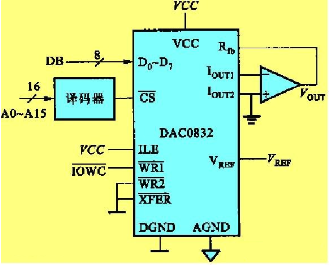
The DAC0832 is an 8-bit resolution D/A converter integrated chip. It is fully compatible with microprocessors. This D/A chip is widely used in microcontroller application systems due to its low cost, simple interface, and easy conversion control. The D/A converter consists of an 8-bit input latch, an 8-bit DAC register, an 8-bit D/A conversion circuit, and a conversion control circuit.
Operating Modes
Based on different control methods for the DAC0832’s data latch and DAC register, there are three operating modes: direct mode, single-buffer mode, and double-buffer mode.
1. Single-buffer mode. In single-buffer mode, the input register and DAC register receive data simultaneously, or only the input register is used while the DAC register is set to direct mode. This mode is suitable for applications with only one analog output or several asynchronous analog outputs.
2. Double-buffer mode. In double-buffer mode, the input register first receives data, and then the output data from the input register is controlled to the DAC register, i.e., the input data is latched in two stages. This mode is suitable for scenarios requiring multiple D/A converters to output synchronously.
3. Direct mode. In direct mode, the data is not latched through two stages of latches, i.e., CS*, XFER*, WR1*, and WR2* are all grounded, and ILE is set to high level. This mode is suitable for continuous feedback control circuits and control systems without microcomputers. However, when using this mode, an additional I/O interface must be connected to the CPU to match the CPU with the D/A conversion. The functional circuit application diagram of the DAC0832 shows that it is an 8-bit D/A conversion chip with a sampling frequency, integrated with two levels of input latches, allowing the DAC0832 chip to have double-buffer, single-buffer, and direct input modes to meet the needs of various circuits (such as requiring multiple asynchronous D/A inputs and synchronous conversions). Therefore, this chip has a wide range of applications. Important information about the DAC0832’s applications is illustrated in the figure below: The D/A conversion result is output in current form. If a corresponding analog voltage signal is required, it can be achieved through a high input impedance linear operational amplifier. The feedback resistor of the op-amp can be referenced through the RFB terminal using the internal inherent resistor or can be connected externally. The logic inputs of the DAC0832 meet TTL levels and can be directly connected to TTL circuits or microcomputer circuits.
Output Form
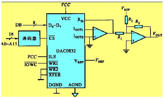
① Unipolar Output. Figure 9-58 shows the unipolar voltage output circuit. It uses an operational amplifier to perform current-to-voltage conversion, utilizing internal feedback resistors. The relationship between the output voltage value VOUT and the input digital value D is: VOUT = – VREF × D/256, D = 0 to 255, VOUT = 0 to – VREF × 255/256, VREF = -5V, VOUT = 0 to 5 × (255/256), VREF = +5V, VOUT = 0 to -5 × (255/256)V.
If the actual application system requires the output analog voltage to be bipolar, a conversion circuit is needed to implement it. Figure 9-59 shows the bipolar voltage output circuit where R2 = R3 = 2R1. VOUT = 2 × VREF × D/256, -VREF = (2D/256 – 1)VREF. When D = 0, VOUT = -VREF; when D = 128, VOUT = 0; when D = 255, VOUT = (2 × 255/256 – 1) × VREF = (127/128)VREF. Thus, when the input digital value is 0 to 255, the output voltage varies between -VREF and +VREF.
The DAC0832 is a D/A conversion chip with two input latches that can be directly connected to the computer bus. Its main features are as follows: 8-bit resolution; single power supply (5—15V); logic input level compatible with TTL levels. The D/A converter output circuit is divided into current output and voltage output types. The voltage output is further divided into unipolar and bipolar types, as shown in Figure 27-11, which illustrates the interface circuit for the DAC0832 unipolar/bipolar voltage output.
In the figure, the data input terminal of the DAC0832 is connected to the data bus of the computer system. The control signals XFER and WR2 are grounded, and ILE is set to high level. When the shorting column KB is shorted between 1 and z, it outputs unipolar voltage (0—10V DC); when KB is shorted between 1 and 4 and 2 and 3, it outputs bipolar (-10V—0—+10V DC).


To help everyone learn better, Changxue Electronics Network has specially added a public account for microcontroller and EDA knowledge, pushing relevant knowledge daily, hoping it can assist your studies!