
1
Background
SiC/GaN is increasingly being applied in designs with higher power and voltage, such as motor drivers for electric vehicles (EVs), fast charging stations for electric vehicles, onboard and offboard chargers, wind and solar inverters, and industrial control power supplies/lighting power supplies. As the switching speed of SiC/GaN power devices increases (extremely high dv/dt), the testing methods and instrument selection principles previously used for Si power devices are no longer suitable for SiC/GaN power devices. Selecting the right oscilloscope to accurately measure the switching characteristics of SiC/GaN and the parameters of the application circuit has become crucial for engineers optimizing circuits.
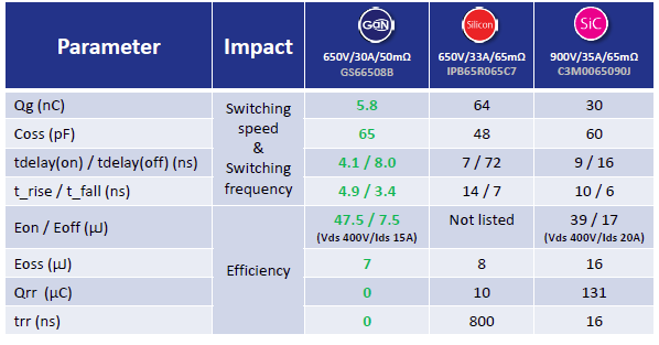
From the above image, it can be seen that the switching speed of SiC/GaN is very fast, and the parasitic parameters are very small.
2
How to Select the Bandwidth/Vertical Resolution/Horizontal Sampling Rate of the Oscilloscope
|
01 |
Oscilloscope Bandwidth |
-
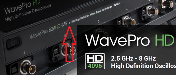
The bandwidth seen on the oscilloscope itself is the -3dB bandwidth of the oscilloscope.
-
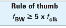
To accurately reflect the signal profile, the oscilloscope bandwidth must be at least five times higher than the frequency of the measured signal.
-
The highest frequency of the measured signal is not its fundamental frequency, but rather the higher harmonics in its rising/falling edges.
|
02 |
Oscilloscope Frequency Response Type |
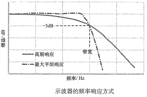
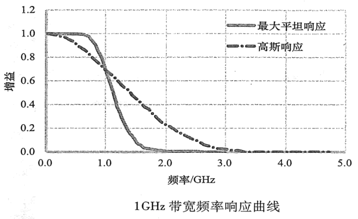
Oscilloscopes with a bandwidth of over 1GHz are typically maximum flat response oscilloscopes:
-
Maximum flat response oscilloscopes exhibit faster roll-off characteristics at -3dB and have a flatter in-band response.
-
In-band signal restoration is more accurate.
-
The rise time (10%-90%) of maximum flat response oscilloscopes is approximately 0.4-0.5/fBW.
Oscilloscopes with a bandwidth of less than 1GHz are usually Gaussian response oscilloscopes:
-
Gaussian response oscilloscopes exhibit slower roll-off characteristics at -3dB.
-
Due to slow attenuation outside the bandwidth, Gaussian response oscilloscopes allow more frequency components to enter the oscilloscope.
-
Under the same bandwidth specifications, Gaussian response oscilloscopes have shorter rise times.
-
The rise time (10%-90%) of Gaussian response oscilloscopes is approximately 0.35/fBW.
|
03 |
Oscilloscope Rise Time |
Rise time is an indicator related to the bandwidth of the oscilloscope:
-
The rise time of the oscilloscope does not indicate the fastest edge speed that the oscilloscope can measure.
-
Rise time refers to the fastest edge speed that the oscilloscope can produce, assuming the rise time of the measured signal is “zero”.
-
In practice, use a fast edge signal that is five times faster than the oscilloscope’s rise time to measure the oscilloscope’s rise time.
-
The rise time (10%-90%) of maximum flat response oscilloscopes is approximately 0.4-0.5/fBW.
-
The rise time (10%-90%) of Gaussian response oscilloscopes is approximately 0.35/fBW.
|
04 |
Oscilloscope Vertical Resolution |
-
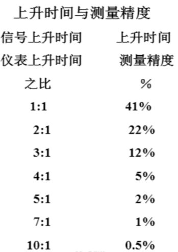
ADC Quantization Bits: In digital oscilloscopes, the ADC converts continuous analog signals into discrete digital signals, determining the vertical resolution of the oscilloscope. The higher the ADC quantization bits, the higher the resolution.
-
Noise and ENOB: Noise originates from the oscilloscope’s analog front end, ADC, probes, cables, etc. Due to noise, the vertical resolution of the oscilloscope is reduced. The quantization bits calculated based on the oscilloscope’s actual achievable resolution are called ENOB. An 8-bit ADC oscilloscope typically has an ENOB of around 6 bits.
For example, measuring a 1200V SiC MOS, if the oscilloscope’s vertical scale is 150V/div, the full scale is 1200V, and the 8-bit ADC resolution is 4.69V, while the ENOB calculation gives a resolution of only 18.75V.

From the above image, it can also be seen that when choosing oscilloscopes from the same series, a sufficient bandwidth is better than a higher bandwidth. For measuring SiC/GaN, a high-resolution oscilloscope should be selected, such as one with a vertical resolution of 12 bits.
|
05 |
Oscilloscope Horizontal Sampling Rate |
-
The sampling rate of Gaussian response oscilloscopes needs to be greater than four times their bandwidth, while the sampling rate of maximum flat response oscilloscopes needs to be greater than 2.5 times their bandwidth.
-
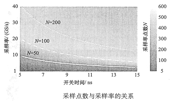
As seen in the right image, the impact of sampling rate on the number of sample points varies with different switching times; shorter switching times require higher sampling rates. For measuring SiC/GaN power devices, a sampling rate of at least 10GS/s is recommended.
-
Due to inherent jitter in oscilloscopes, one should not blindly pursue high sampling rates; the principle of sufficiency should also apply to sampling rates.
|
06 |
Knee Frequency |
-
In the spectrum of fast edges, there is a turning point called “Knee frequency”; frequency components above fknee can be ignored when determining the signal shape.
-
The calculation of Knee frequency is shown in the right image.
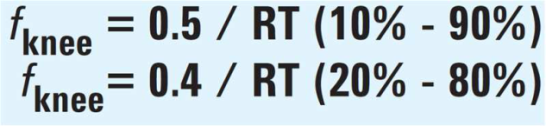
Here, RT 10%-90% and RT 20%-80% refer to the rise times defined by the measured signal’s rising edge amplitude of 10%-90% and 20%-80%, respectively. The higher the oscilloscope bandwidth above the Knee frequency, the higher the measurement accuracy of the rise time.
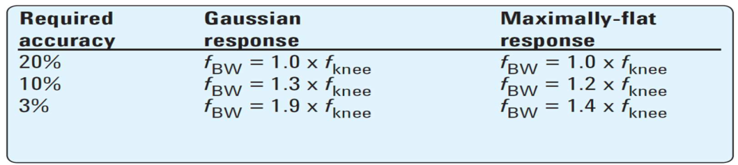
Determine the required bandwidth of the oscilloscope based on different testing precision requirements.
Select an appropriate bandwidth oscilloscope based on the Knee frequency.
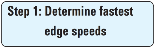
Step 1: Confirm the fastest rise time of the measured signal.
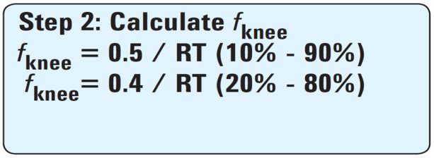
Step 2: Calculate the Knee frequency based on the fastest rise time of the measured signal.
Step 3: Determine the minimum bandwidth of the oscilloscope based on the Knee frequency.
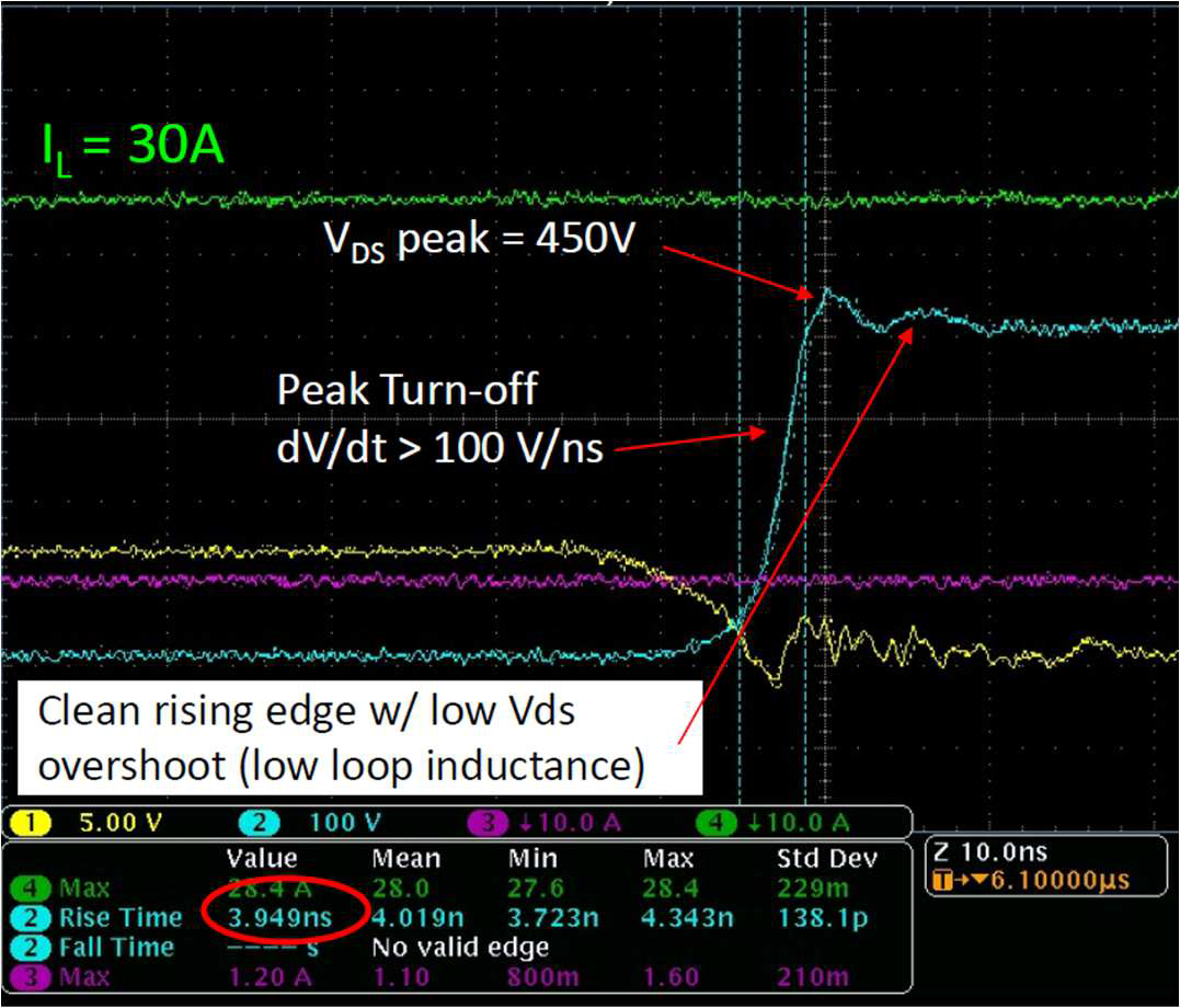
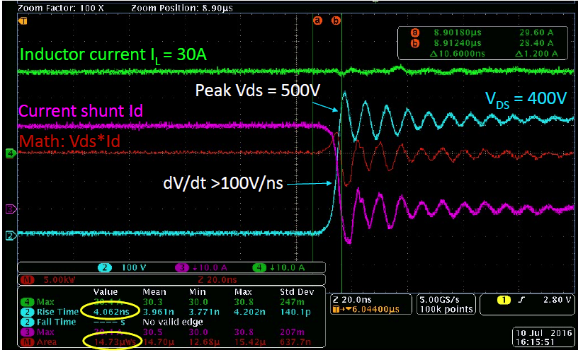
A measured GaN MOS turn-off waveform.
|
07 |
Example Explanation |
-
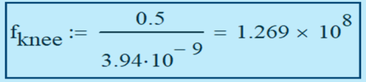
The rise time of GaN’s Vds is approximately 3.94ns.
-
If using a 125MHz bandwidth oscilloscope, the measurement error of Vds may be around 20%. To achieve a 3% error, at least a 250MHz bandwidth oscilloscope and probe are required.
Above only considers the bandwidth of the oscilloscope, while the measurement system consists of both the oscilloscope and probes, requiring consideration of the overall bandwidth of the measurement system. The system bandwidth and rise time of Gaussian response oscilloscopes are calculated using the following two formulas:
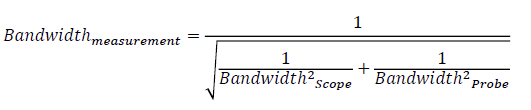
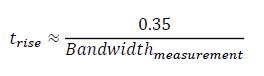
Probes also have rise times and bandwidths, and typically the testing bottleneck of the entire system lies in the bandwidth of the probes.
In a bridge topology, measuring the high-voltage differential probe of the upper MOS requires at least 400M bandwidth.
The oscilloscope should have at least a vertical resolution of 12 bits and a bandwidth of 350M.
For example: Tektronix MSO44
Lecroy HDO4034A
3
How to Select Voltage Probes/Current Probes
Voltage Probes:
-
Low-voltage passive probes: at least 300M bandwidth; if using a 350M oscilloscope, the included probes will suffice.
-
High-voltage differential probes: at least 400M bandwidth, with high CMRR and input impedance requirements.
BumbleBee® Differential HV-Probe
■ 400MHz bandwidth■ ±2000V differential input voltage range■ 1000V CAT III input voltage range■ CMRR up to 80dB ■ Switchable dividing stages 50X/100X/250X/500X for lowest noise in the required voltage range■ Universal use with any oscilloscope with 50Ω input■ DC offset correction up to ±4V (output related)
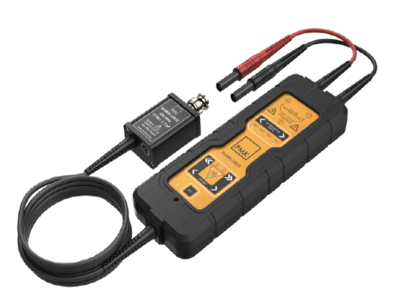
DP0001A 400 MHZ High Voltage Differential Probe
■ 400 MHz bandwidth
■ 2,000 Vrms main power isolation, 6,000 V transient overvoltage protection
■ Attenuation ratio: 50:1, 100:1, 250:1, or 500:1, can automatically switch on Infiniium oscilloscopes
■ Differential input impedance: 10 MΩ || 2pF
■ High common mode rejection ratio: >90 dB from DC to >10 MHz in 500:1 mode; >70 dB at up to 400 MHz
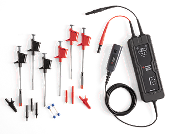

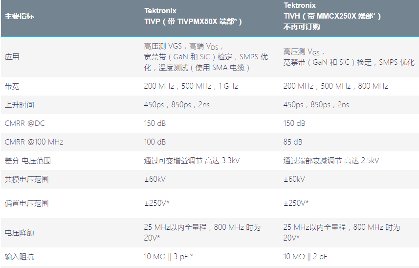
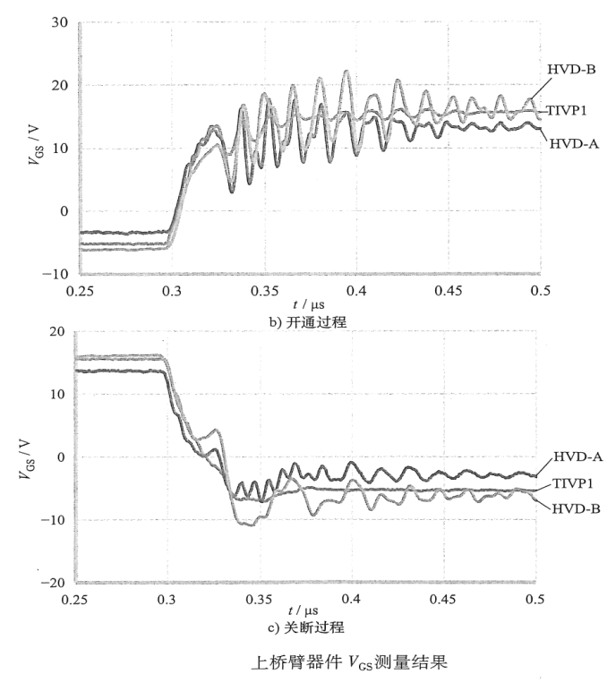
Figure 1: A comparison of waveforms measured using an optical isolated probe (TIVP1) and a certain brand of 120M/80M high-voltage differential probe (HVD) shows that the waveform measured by a low-bandwidth high-voltage differential probe is severely distorted.
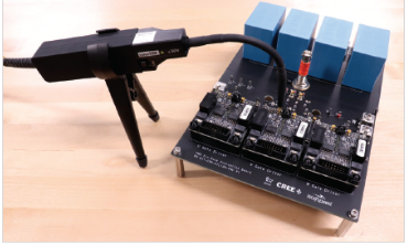
Figure 2: The TIVP system also provides MMCX connectors, adapters to MMCX, and pointed sensor tip cables to reduce parasitic parameters and interference in probe connections.
Current Probes
In addition to the commonly used active current probes (Hall probes, which can measure AC/DC currents), there are two other types of current probes that can also be used:
Coaxial Sampling Resistor
Advantages: high bandwidth, high testing accuracy.
Disadvantages: increases loop parasitic inductance, larger size.
Suitable for Eon/Eoff testing, high-precision current measurement.
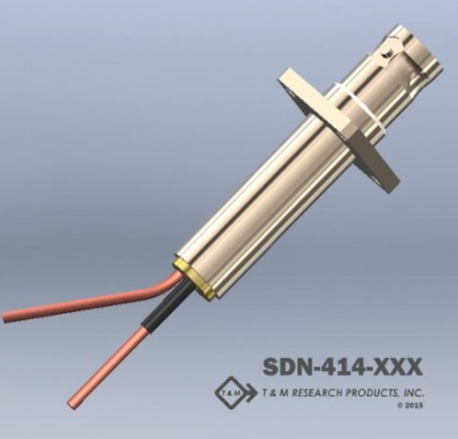
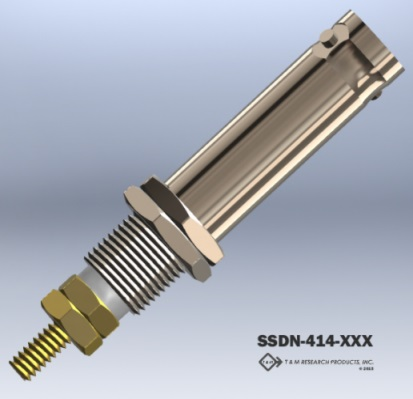
T&M Research co-axial current shunt
• SDN-414-10 (0.1Ω, 2GHz bandwidth)
• SSDN series for low insertion inductance.

Rogowski Coil
Advantages: isolated output, low insertion loop parasitic inductance, small size.
Disadvantages: low bandwidth, not suitable for switching energy measurement.
Suitable for high current testing.
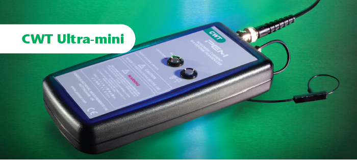
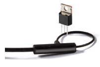
PEM CWT Ultra Mini
• 30MHz, 300A—6000A.
4
Measurement Precautions
|
01 |
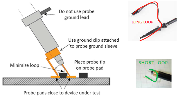
The measurement ground loop must be small. |
|
02 |
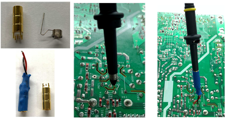
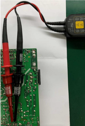
The ground loop for measurement shown in the figure below must be small. |
|
03 |
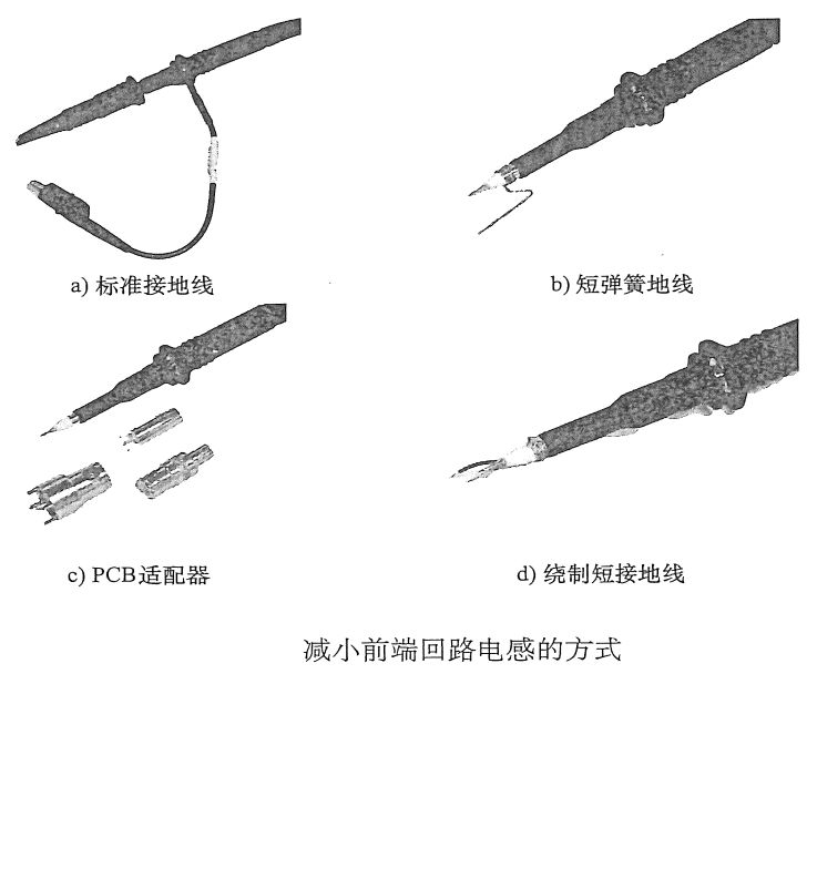
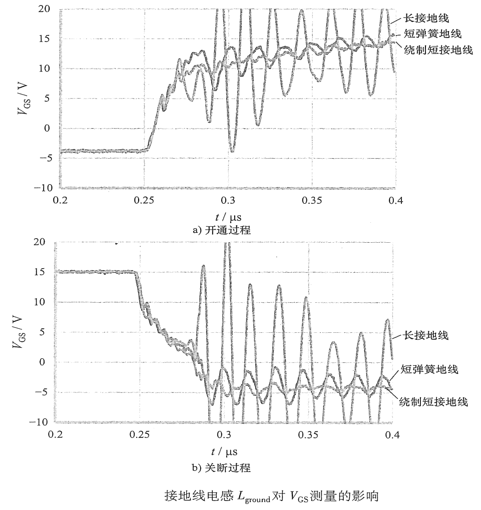
Measurement distortion caused by different grounding wire inductances. |
|
04 |
High Voltage Differential Probes |
-
For voltage measurements of GaN/SiC with high dv/dt, it is not recommended to use isolation transformers to float the oscilloscope ground.
-
The bandwidth/rise time of high-voltage differential probes must meet the requirements.
-
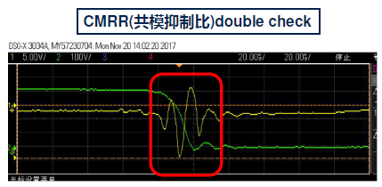
It is necessary to confirm the common mode rejection ratio of the differential probes, especially for probes that have not been calibrated for a long time. Connect the positive and negative terminals of the differential probe to the midpoint of the half-bridge and observe whether the differential probe can detect the common mode signal during instantaneous voltage changes at the midpoint.
-
Differential probes should also be placed in twisted pairs to reduce probe loops.
|
05 |
Probe Time Delay Calibration |
In addition to having sufficient bandwidth and noise suppression capabilities, the probes used must also undergo time delay calibration to ensure that the voltage and current signals are time-matched. If the time delays of the voltage probes and current probes are mismatched by even 1-2ns, it can lead to measurement errors in Eon and Eoff of 30% or more. Proper time delay calibration is crucial for measuring the inherent fast switching transient signals in SiC/GaN systems. The figures show a significant difference in the turn-on and turn-off energy measurements before and after calibration:
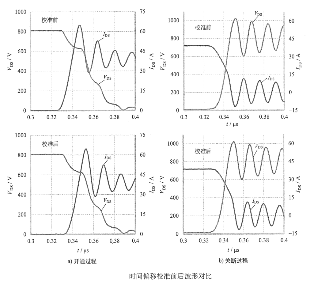
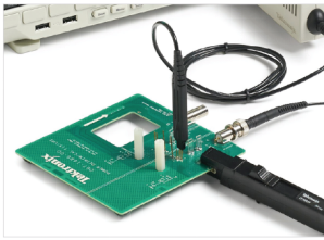
Time delay calibration and calibration fixtures for power measurement probes.
|
06 |
Oscilloscope Sampling Rate and Memory Depth |
-
The sampling rate is represented in samples per second (S/s), indicating the frequency at which the digital oscilloscope captures signal snapshots or samples, similar to camera frame rates. The higher the oscilloscope’s sampling rate, the higher the resolution and displayed waveform details, and the lower the likelihood of missing key information.
-
Nyquist’s theorem states that the signal sampling rate must be at least twice the highest frequency component of the measured signal. However, this theorem assumes infinite recording length and that the measured signal is continuous. For oscilloscope engineering applications, two times is usually not enough.
-
For oscilloscopes using sin(x)/x interpolation, the sampling rate should be at least 2.5 times the highest frequency of the measured signal.
-
For oscilloscopes using linear interpolation, the sampling rate should be at least 10 times the highest frequency of the measured signal.
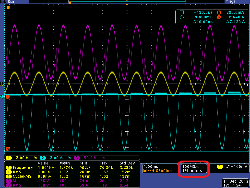
Memory depth = time range x sample rate.
|
07 |
Set Appropriate Sampling Rate and Time Base |
-
Increasing the oscilloscope’s memory depth can indirectly increase the oscilloscope’s sampling rate: when measuring longer waveforms, the memory depth is fixed, so the sampling rate can only be reduced to achieve this, which inevitably leads to a decline in waveform quality. If the memory depth is increased, it allows for a higher sampling rate to measure without distortion.
-
For the same GaN MOS turn-off waveform, if the rise time of the measured signal is 4.9ns, the sampling interval should not exceed 490ps, and the minimum sampling rate should be around 2GS/s.
-
If the oscilloscope’s memory depth is 10MS, to achieve a small sampling interval, the maximum recording time length of the oscilloscope is approximately 5ms. Typically, the oscilloscope’s horizontal axis has ten divisions, so the time base is approximately 500us/div.
(PS: Assume this oscilloscope’s maximum sampling rate is exactly 2GS/s, then a time base of less than 500us/div will not help the waveform quality.)
|
08 |
Bandwidth Settings |
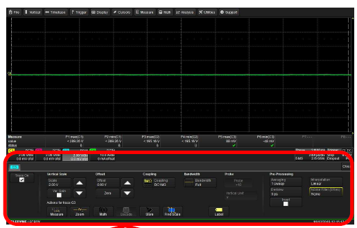
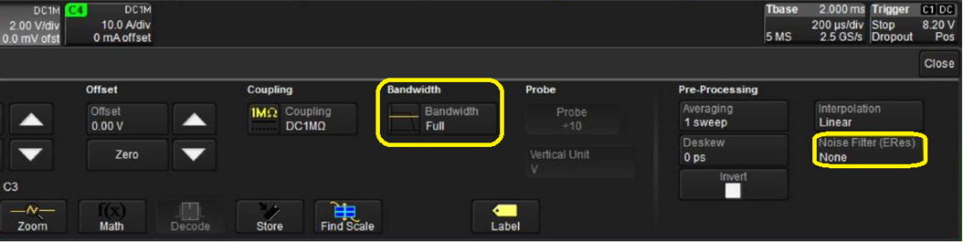
-
Bandwidth: Set to full bandwidth.
-
Noise Filter: No filtering needed.
Weiyali Electronics is a well-known electronic component distributor, representing the full range of ST (STMicroelectronics) products, including SiC/GaN. The company’s application engineer team has extensive design and testing experience in SiC/GaN product applications and is fully capable of assisting customers in efficiently completing various circuit designs.
Brain Challenge, Real-time Lottery for Prizes. Scan the code to participate in the prize-winning activity after reading, answer three questions correctly to enter the grand lottery, and win a Weiyali 40th Anniversary Wireless Power Bank.
Event Time: 2022.4.1 – 4.8
Announcement of Winners: 2022.4.13
Warm Reminder: Winners should send their winning screenshots, names, phone numbers, and addresses to the public account. We will collect them and distribute them uniformly after completion.
Tips
The Weixingren 40th Anniversary Emoji Pack
40th Anniversary Emoji Pack is now online.
Quickly use it with your friends.
Show it off in your circle of friends!
The editor believes that those using the Weixingren Emoji Pack will definitely become the coolest surfers online!
Click the menu “Weixingren Emoji Pack” to receive the exclusive emoji pack for Weiyali people!