Source: Tianlang Semiconductor
Recently, Tianlang Semiconductor achieved a significant breakthrough in the research and development of SiC shallow junction MOS chips. The design scheme of this SiC shallow junction MOS has led to a remarkable improvement in product performance under the technical conditions where the JFET and junction depth are at their limit, with a breakdown voltage (BVDSS) reaching 1670V and a specific on-resistance (RSP) of 2.4mΩ·cm². These technical indicators have successfully surpassed the levels of similar products disclosed by STMicroelectronics (STM) and Wolfspeed, and the product has now smoothly transitioned into mass production.
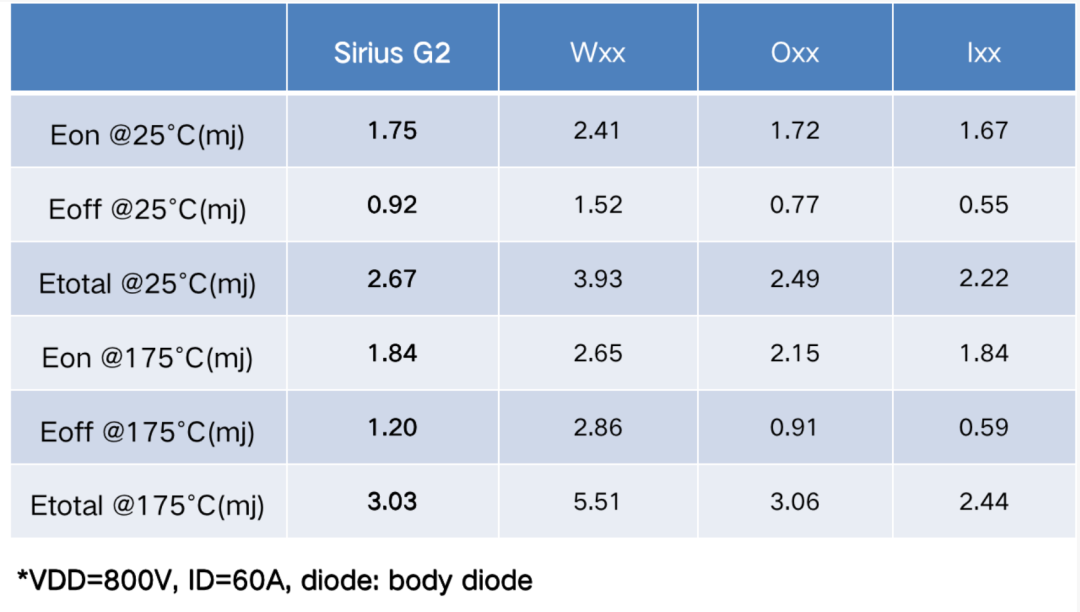
This milestone not only marks a new level of technological strength in China’s SiC chip field but also provides more efficient and reliable core component solutions for numerous industries, including new energy vehicles, photovoltaic power generation, and smart grids.
Notably, the shallow junction chip from Tianlang Semiconductor has reduced the on-resistance by 40% compared to the previous generation and has overcome the key core issue of shallow junction technology—leakage issues. Testing shows that the leakage current (Idss) of this generation of shallow junction products can be stably controlled within 20nA, reaching the first-tier level in the industry. This means that the chip can operate with lower power consumption and higher efficiency, providing customers with an excellent user experience across multiple application scenarios, further promoting technological upgrades and cost optimization in related industries.
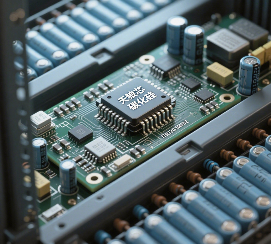
Wide Application, Supporting Upgrades in Multiple Fields
01
Energy Storage Sector
As global demand for renewable energy continues to grow, the importance of energy storage systems is becoming increasingly prominent. Tianlang Semiconductor’s SiC shallow junction MOS series products, with their efficient and stable performance, can effectively enhance the charge and discharge efficiency of energy storage systems, extend battery life, and inject new vitality into the energy storage industry.
02
New Energy Vehicle Main Drive
In the field of new energy vehicles, the performance of chips directly affects the vehicle’s power performance and range. Tianlang Semiconductor’s chips feature high voltage resistance, low resistance, and high EAS impact resistance, significantly reducing energy loss in the main drive system, enhancing vehicle power output and energy utilization, and helping the new energy vehicle industry reach new heights.
03
New Energy Vehicle Charging Piles
High-power DC fast charging has become a development trend in the charging pile industry. Tianlang Semiconductor’s SiC shallow junction MOS series products can meet the high power and high efficiency requirements of charging piles, achieving faster charging speeds and reducing user waiting times, providing strong support for the development of the charging pile industry.
04
OBC (On-Board Charger)
As an important component of new energy vehicles, the performance requirements for chips in OBC are extremely high. Tianlang Semiconductor’s SiC shallow junction MOS series products can effectively improve the conversion efficiency of OBC, reduce heat generation, and enhance system reliability and stability. Company Profile
Tianlang Semiconductor Technology (Shanghai) Co., Ltd. was established in 2021, with core team members coming from international semiconductor giants such as TSMC, MediaTek, and Broadcom, averaging over 15 years of experience in the semiconductor industry, with a deep understanding of semiconductor chip design and wafer manufacturing processes. Relying on resource integration and technological innovation, the company is committed to the development of high-quality, high-reliability power semiconductor products, mainly including MOSFETs, IGBTs, SiC, and GaN series wide bandgap power semiconductor devices, which are widely used in new energy generation, new energy vehicles, rail transit, smart grids, photovoltaic energy storage, consumer electronics, and other fields. Starting in 2023, Tianlang Semiconductor is gradually transitioning from a fabless model to a fablite model through vertical integration of industry chain resources.
In late 2023, the company established an automotive-grade reliability testing center in Jiading District, Shanghai. This testing center is a key open experimental platform for power devices that Tianlang Semiconductor is focusing on building, mainly engaged in reliability testing and verification of automotive-grade power devices (MOSFET, SiC, GaN, IGBT single tubes + modules), dedicated to providing reliability testing and certification reports for Tianlang and its customers.
In terms of end products, Tianlang Semiconductor is further laying out GaN PD fast charging products, which use self-developed GaN chips with the lowest lattice mismatch, ultra-fast switching frequency, and perfect thermal expansion coefficient, giving fast charging products unparalleled advantages in performance. Mr. Zeng Jianzhong, the founder of Tianlang Semiconductor, expressed great expectations for the development of more applications of GaN in industrial, automotive, and consumer electronics fields, including Tianlang Semiconductor’s 650V GaN products, which have already entered mass production in the PD fast charging market, with applications in 65W, 90W, 140W, and 200W products recognized by the market; products with 1200V specifications have also begun small batch testing in the high-voltage lithium battery 800V to 48V/12V applications for new energy vehicles. Tianlang Semiconductor’s related products have been successfully introduced to internationally renowned companies such as State Grid, Hyundai Motor, Ford, Huawei, and Honor.