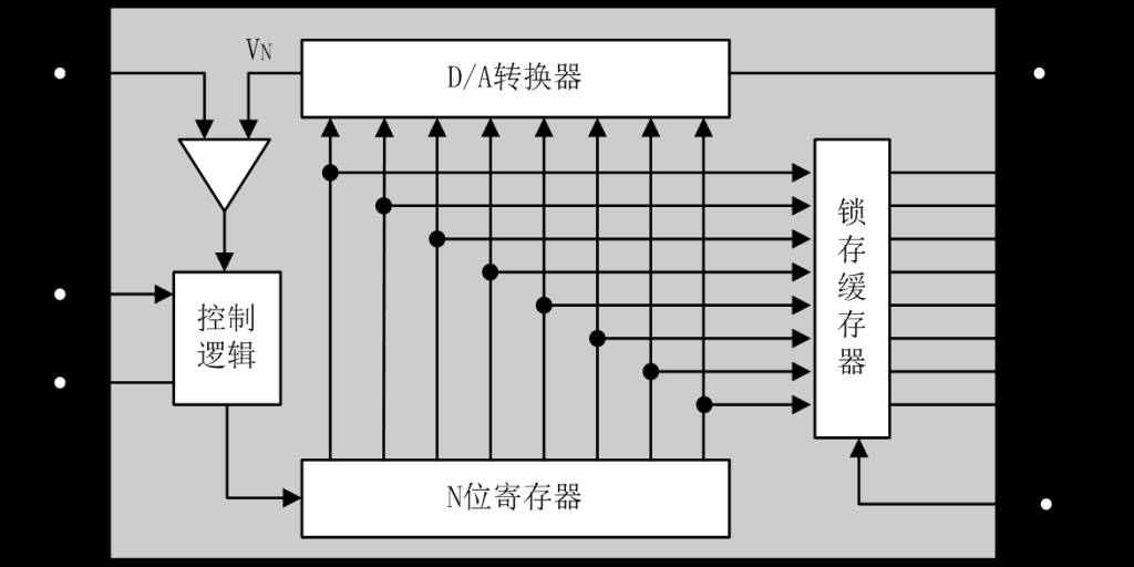
1. Basic Principles and Classification of D/A Converters
T-type Resistor Network D/A Converter:
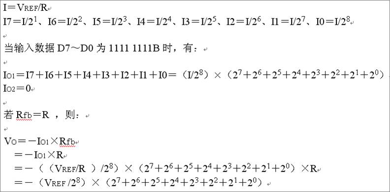
2. Correspondence between Output Voltage and Digital Quantity
3. Main Performance Indicators of D/A Converters
1. Resolution
Resolution refers to the change in the corresponding output analog quantity (voltage or current) when the least significant bit (LSB) of the input digital quantity changes. It reflects the minimum change value of the output analog quantity.
The resolution has a definite relationship with the number of bits in the input digital quantity, which can be expressed as FS / 2^n. FS represents the full-scale input value, and n is the number of binary bits. For a 5V full scale, using an 8-bit DAC, the resolution is 5V/256=19.5mV; when using a 12-bit DAC, the resolution is 5V/4096=1.22mV. Clearly, the more bits, the higher the resolution.
2. Linearity
Linearity (also known as non-linearity error) is the maximum deviation between the actual conversion characteristic curve and the ideal straight line characteristic. It is often expressed as a percentage relative to the full scale. For example, ±1% means that the difference between the actual output value and the theoretical value is within ±1% of the full scale.
3. Absolute Accuracy and Relative Accuracy
Absolute accuracy (abbreviated as accuracy) refers to the maximum error between the actual output value of the analog quantity corresponding to any input digital code and the theoretical value across the entire scale range. Absolute accuracy is caused by the DAC’s gain error (the difference between the actual output value and the ideal output value when the input digital code is all 1s), zero error (the non-zero output value of the DAC when the digital input is all 0s), non-linearity error, and noise, etc. The absolute accuracy (i.e., maximum error) should be less than 1 LSB.
Relative accuracy expresses the same meaning as absolute accuracy, represented as the maximum error relative to the full scale as a percentage.
4. Settling Time
Settling time refers to the time required for the output analog signal to reach ±1/2 LSB of the full-scale value when the input digital quantity undergoes a full-scale change. It is a dynamic indicator describing the D/A conversion rate.
The settling time of current output DACs is short. The settling time of voltage output DACs is mainly determined by the response time of the operational amplifier. Based on the length of the settling time, DACs can be divided into several categories: ultra-high speed (<1μS), high speed (10~1μS), medium speed (100~10μS), and low speed (≥100μS).
It should be noted that accuracy and resolution are related, but the concepts are different. When the DAC has many bits, the resolution will improve, and the quantization error affecting accuracy will decrease. However, the impact of other errors (such as temperature drift, poor linearity, etc.) will still degrade the accuracy of the DAC.
4. Chip Examples
1: DAC0832
The DAC0832 is a widely used 8-bit D/A converter. Since it has an internal input data register, it can be directly interfaced with microcontrollers. The DAC0832 outputs in current form, and when conversion to voltage output is needed, an operational amplifier can be connected externally. Other chips in this series include DAC0830 and DAC0831, which can be interchanged. Main features of DAC0832:
Resolution: 8 bits;
Current settling time: 1μS;
Data input can use double buffering, single buffering, or direct mode;
Output current linearity can be adjusted at full scale;
Logic level input is compatible with TTL levels;
Single power supply (+5V~+15V);
Low power consumption, 20mW.
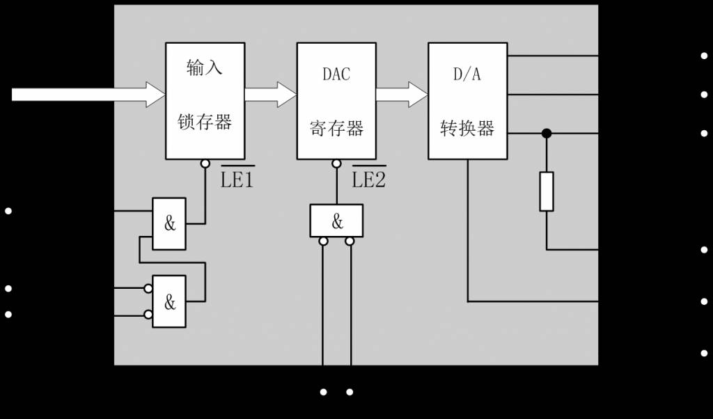
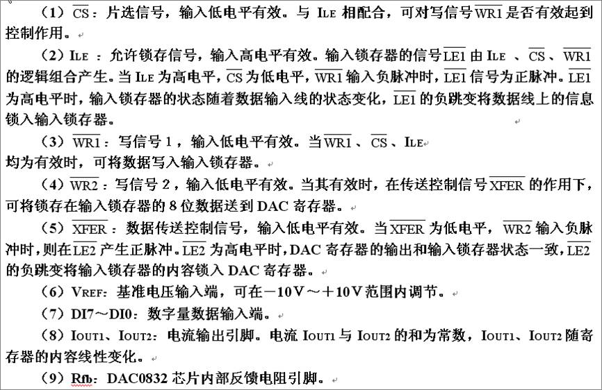
Pin Description:
2: Three Operating Modes of DAC0832
1. Single Buffer Operating Mode
This mode is suitable for systems with only one analog output or several analog outputs that do not require synchronization.
That is: default CS = XFER = 0, ILE = 1; WR is controlled separately. Buffering is controlled solely by WR.
1.1 Unipolar Analog Output
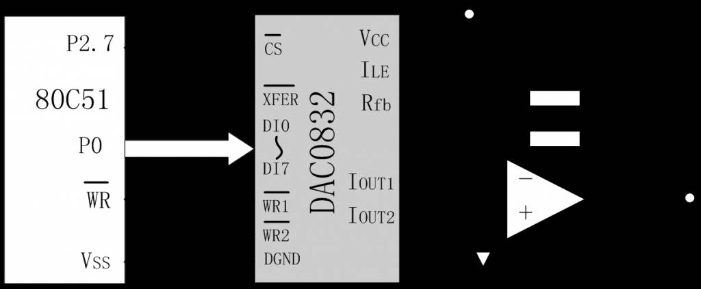
1.2: Bipolar Analog Output Voltage
The resolution for bipolar output is reduced by 1/2 compared to unipolar output, since for bipolar output, the highest bit serves as the sign bit, leaving only 7 bits for the value.
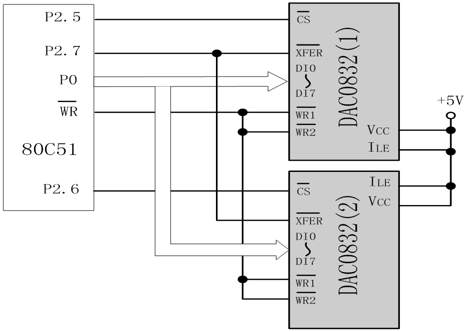
2. Double Buffer Operating Mode
If multiple D/A conversion outputs require synchronization, the double buffer synchronization method should be used.
That is: default CS = 0, ILE = 1; WR and XFER are controlled separately, buffering is controlled by both WR and XFER.
3. Direct Mode
When the chip select signal CS, write signal WR, and transfer control signal XFER pins of the DAC0832 chip are all grounded, and the input latch signal ILE pin is connected to +5V, the DAC0832 chip operates in direct mode, where the digital quantity is directly entered into the DAC register for D/A conversion.
That is: CS = WR = XFER = 0, ILE = 1;
A/D Converters
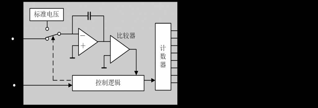
1. Successive Approximation ADC Conversion Principle
2. Dual-Slope ADC Conversion Principle
3. Main Technical Indicators of A/D Converters
1. Resolution
The resolution of an ADC refers to the change in the input analog voltage required to change the output digital quantity by one adjacent code. It is commonly expressed in terms of binary bits. For example, a 12-bit ADC has a resolution of 12 bits, or the resolution is 1/ 2^n of the full scale FS. A 12-bit ADC with a 10V full scale can resolve the minimum input voltage change of 10V×1/ 2^12 =2.4mV.
2. Quantization Error
Quantization refers to the process of converting an analog quantity into a digital quantity, where the digital quantity approximates the analog quantity. The quantization error is the error caused by the ADC’s finite number of bits quantizing the analog quantity. In reality, to accurately represent the analog quantity, the ADC’s number of bits needs to be very large or even infinite. The maximum deviation between the step-like conversion characteristic curve of a limited resolution ADC and the conversion characteristic curve (line) of an ADC with infinite resolution is the quantization error.

3. Offset Error
Offset error refers to the value of the output signal when the input signal is zero, so it is sometimes referred to as zero error. Assuming the ADC has no non-linear error, the line connecting the midpoints of each step in the conversion characteristic curve must be a straight line. The intersection point of this line with the horizontal axis corresponds to the input voltage value of the offset error.
4. Full Scale Error
Full scale error, also known as gain error, refers to the difference between the actual input voltage corresponding to the full-scale output code and the ideal input voltage.
5. Linearity
Linearity, sometimes referred to as non-linearity, refers to the maximum deviation between the actual conversion characteristics of the converter and the ideal straight line.
6. Absolute Accuracy
The maximum value of the difference between the actual analog input corresponding to any code in a converter and the theoretical analog input is called absolute accuracy. For ADCs, it can be measured at the horizontal midpoint of each step, including all errors.
7. Conversion Rate
The conversion rate of an ADC is the speed at which it can repeatedly perform data conversions, i.e., the number of conversions per second. The time required to complete one A/D conversion (including stabilization time) is the reciprocal of the conversion rate.
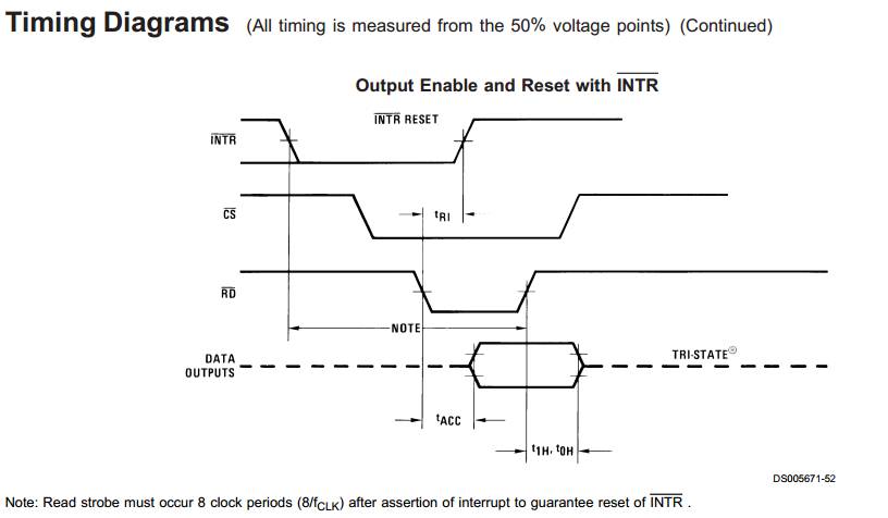
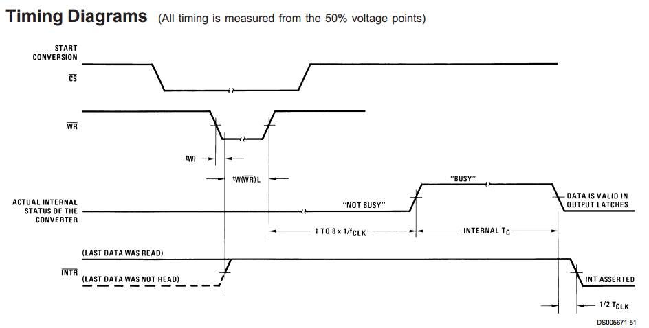
4. AD080X Demo
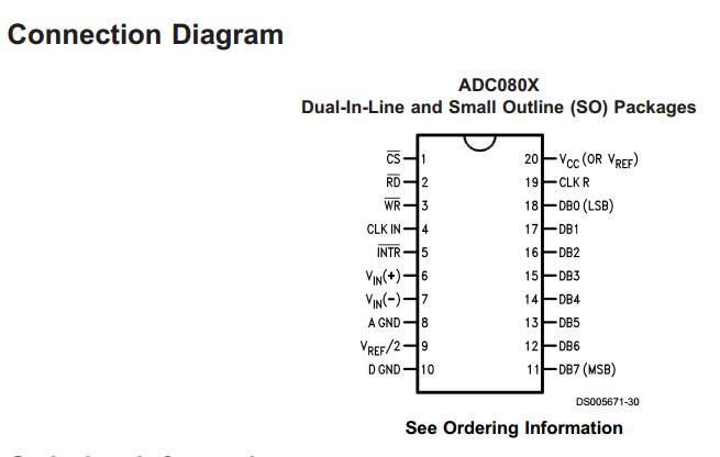
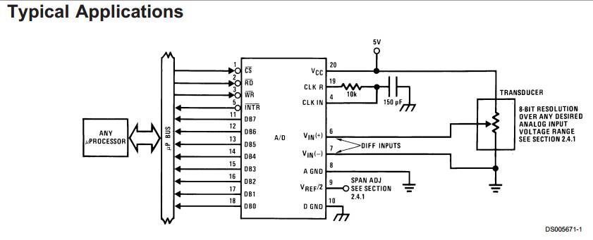
PIN5 If using interrupt mode to notify the CPU, connect to the external interrupt; otherwise, 5 can be left unconnected, and delay can be read directly.
The startup timing diagram is as follows:
Code demo:
void Launch()
{
    CS = 0;
    WR = 1; WR = 0; WR = 1;
    /*Waiting for INTR goto 0*/
}
Reading Timing Diagram:
Code demo:
void ReadAD()
{
    /* INTR had goto 0*/
    CS = 0;
    RD = 1; RD = 0; /*delay*/ RD = 1;
    /* READ */
}