
PCB Network News

01
What is a Core Board?
SUNSHINE GLOBAL CIRCUITS
SOMs are suitable for various industries including industrial automation, medical devices, automotive electronics, communication systems, and the Internet of Things (IoT). Using SOMs can greatly shorten product development cycles, reduce overall costs, and improve product reliability.
02
Classification of Core Boards
SUNSHINE GLOBAL CIRCUITS
To ensure the compatibility, modularity, and scalability of embedded core board hardware and software, different organizations or companies have defined multiple standards. The common embedded core board standards are as follows:
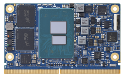
Open Standard Module (OSM)
OSM core boards are solderable LGA package modules with a compact size, with a maximum dimension of 45mm x 45mm, and module power typically below 15W. They are very friendly for IoT applications, meeting low-cost and increasing performance demands.
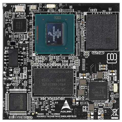
OSM standard IMX8MP core board
From: ADLINK
QSeven (Q7)
A standard for embedded processor modules based on ARM architecture introduced by NXP Semiconductors (formerly Freescale Semiconductor). The standard uses a 230-pin MXM gold finger design, facilitating high-speed I/O connections in handheld devices, HMIs, and signage applications.
SMARC
SMARC (Standard Module Advanced RISC Computer) is an open standard for defining embedded computer modules based on ARM architecture. It uses a 314-pin MXM gold finger connector, suitable for products with high performance and low power requirements.
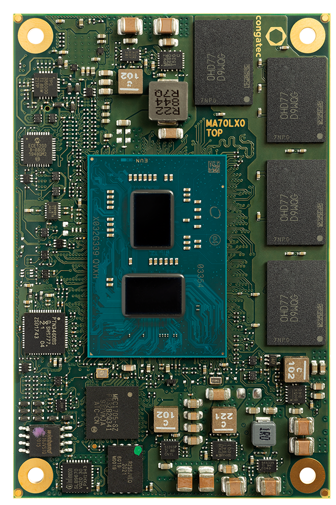
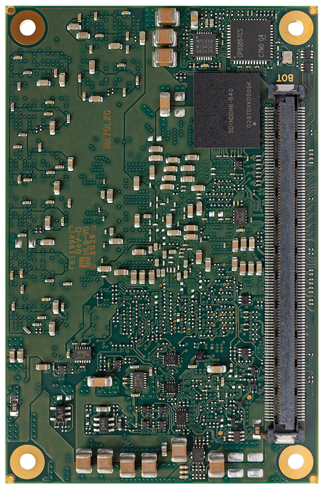
COM Express
A modular computer standard defined by PICMG (PCI Industrial Computer Manufacturers Group) that supports multiple processor architectures such as x86, ARM, and PowerPC. COM Express modules include Mini, Basic, and Compact sizes, which can be selected based on specific applications and power requirements.
To accommodate the next generation of AIoT applications, COM Express R3.1 has added multiple advanced interface supports including Type 6/7/10 with new PCIe Gen 4 interfaces, Type 6 modules with additional USB 4.0 interfaces, Type 7 modules with an additional PCIe Clock, and upgraded 10G Ethernet to support CEI sideband signals.
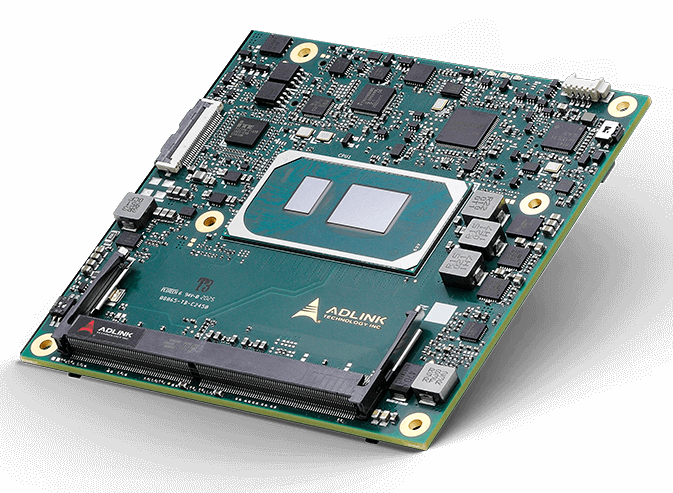
COM Express Type 6 11th Gen Intel Core i7 Core Board
From: ADLINK
03
PCB Design of Embedded Core Boards
SUNSHINE GLOBAL CIRCUITS
As embedded processors become more powerful and memory speeds increase, the number of PCB layers in embedded core boards has evolved from the early 4 layers to 8-12 layers. This is due to the increasing number of high-speed interfaces and higher requirements for board material loss.
Generally, the following steps are followed in the design of embedded core board PCBs:
Determine Component Layout
Generally speaking, the core board standards have already specified the standard shape and interfaces, so the layout of components does not change much. The general approach is to follow the optimal fanout layout design according to the CPU reference manual requirements, determine the layout of the CPU, DDR, and Flash, and then optimize the layout of the power supply and surrounding components.
Determine Board Thickness
The common PCB finished thicknesses are 0.5mm, 0.8mm, 1.0mm, 1.2mm, 1.6mm, 2.0mm, 3.2mm, 6.4mm, etc. The core board design standards usually specify the board thickness, and it is necessary to follow the corresponding requirements. For those without specified requirements, it can be made thicker from the perspective of structural reliability.
Determine PCB Layer Count and Functional Layer Division
Determine the total layer count and divide signal layers, power layers, and ground layers, which requires a comprehensive consideration from a systemic perspective and is a result of mutual compromise. First, it is necessary to determine that the layer count can meet the wiring requirements, secondly to meet the wiring requirements of high-speed signal lines, and finally to consider the requirements of power integrity, EMC, and thermal design. While meeting functional requirements, try to minimize the number of PCB layers.
Determine Inner and Outer Layer Copper Thickness
In layered design, it is necessary to balance the thickness of the copper foil to ensure that the copper thickness of the power/ground plane meets the current-carrying requirements. Copper thickness above 3oz is considered thick copper and is commonly used in high-voltage, high-current power electronic products.
For the copper thickness of signal layers, the line width/line spacing is relatively small, and the copper needs to be as thin as possible to meet precise etching requirements. Due to the skin effect, high-speed signal lines only flow near the surface of the copper foil, so thicker copper foils do not provide better performance. Therefore, the copper thickness of the inner signal layer is usually Hoz, which is 0.5 ounces.
Determine Impedance Line Distribution
High-speed interface signal lines on core boards have impedance requirements, commonly single-ended 50Ω, differential 100Ω, etc. Impedance control requires a reference plane, and the copper thickness, dielectric constant, line width, and line spacing will all affect impedance. When designing impedance lines, try to minimize the number of layers where impedance lines appear while meeting impedance requirements.
EDA tools support impedance calculations, which can adjust the wiring parameters according to the designed layering structure.
Determine Via Structure
Most core boards use blind and buried vias to optimize wiring space due to their high-density properties. However, blind and buried vias also increase the manufacturing difficulty of PCBs due to multiple pressings, making them more expensive.
When designing layers, it is necessary to simplify via structures as much as possible while meeting design requirements.
Select Board Materials, PP, and Copper Foil that Meet Design Requirements
FR-4 can meet the needs of most PCBs, being inexpensive and having good electrical performance. High-speed PCBs will select high-speed materials, such as Panasonic’s Megtron4/6, etc., which require dielectric materials with the lowest loss tangent and a smaller dielectric constant to meet the loss requirements of high-speed signals.
The roughness of copper foil (copper teeth) can cause uneven line width and line spacing, leading to uncontrollable impedance. At the same time, due to the skin effect, the current concentrates on the surface layer of the conductor, and the surface roughness of the copper foil affects the signal transmission length. The impact of copper foil roughness is not very noticeable when the signal frequency is below 5GHz, but it becomes increasingly significant above 5GHz, especially for high-speed signals above 10GHz.


