Introduction
RAM is the component in a computer system that stores temporary results, and its size also determines the scale of data processing by the computer. In embedded computers (microcontrollers), due to factors like cost and power consumption, the internal RAM capacity is often quite small, typically ranging from a few hundred bytes to several kilobytes. This is sufficient for most microcontroller applications.
However, in some special applications, a large capacity of RAM is sometimes required to store collected data or buffer communication data. In such cases, external memory expansion is necessary. For example, recent experiments related to sound beacon signal systems require the collection of multiple audio signals. Thus, external RAM expansion is needed.
The interface of static RAM chips generally includes data, address, and control buses, which can be connected to the corresponding ports of the microcontroller to facilitate data writing and reading.
Some microcontrollers, when expanding external RAM, use external latches to multiplex the same eight-bit address port to achieve a 16-bit address bus, in order to save limited IO ports. For example, the 8051 microcontroller. The trade-off for this design is the need to add an external latch chip, such as the 74LS372.
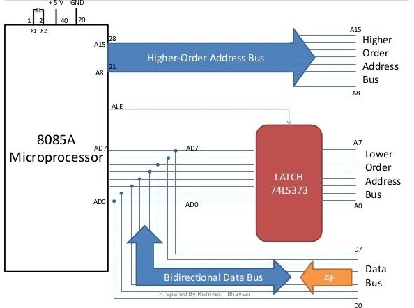
Although the data bus and address bus are logically marked with the order of data bits: for example, a 16-bit address bus labeled A0~A15 and an 8-bit data bus denoted D0-D7. However, when accessing static RAM, the order of these bits within the data bus and address bus can be adjusted arbitrarily.
For instance, in the microcontroller system designed below, the order of the internal bits of the data bus and address bus is adjusted to minimize PCB wiring crossovers.
Expanding External 32KB RAM for STC8H8K
1. Design Description
The STC8H8K microcontroller has a 16-channel 12-bit ADC, which is used in this experiment to collect the Chirp sound emitted by the beacon and transmit it to a computer for processing.
The blog post “High-Speed ADC Collection Board Based on STC8G8K64U” provides a design scheme for collecting sound signals using the internal 8KB RAM of the STC8H8K. However, due to the space limitation of the internal 8KB RAM, the number of audio signals that can be collected and the duration cannot meet the research objectives. Therefore, this time, we expand with an additional 32KB SRAM to increase the signal collection capacity.
Similarly, a WiFi-UART conversion module is used to achieve data transmission between the collected data and the PC, consistent with the design scheme in the previous blog post.
2. Schematic Diagram
The STC8H8K chip is packaged in TSOP48. The P2 port is used as data summary, while P0 and P4 ports are used as the address bus. No external latches are required.
UART3 is used for communication with the WiFi-UART module. The AD0~AD2 from the ADC are routed to the input ports to receive the externally collected signals.
The specific circuit diagram is shown below:
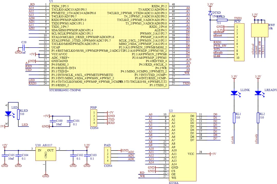
External interface design:
(1) ISP Port:
| No. | Symbol | Function |
|---|---|---|
| 1 | VCC | +5V Power Supply |
| 2 | GND | Ground |
| 3 | TXD | MCU Serial Output |
| 4 | RXD | MCU Serial Input |
(2) ADC Port:
| No. | Symbol | Function |
|---|---|---|
| 1 | ADC0 | ADC Channel 0 |
| 2 | ADC1 | ADC Channel 1 |
| 3 | ADC2 | ADC Channel 2, can also be used as a general IO |
2. PCB Board
It should be noted that in order to adapt to the needs of rapid prototyping, a single-sided PCB process was used. To eliminate crossover in wiring (as crossover requires vias and double-sided wiring), the order of the data bus and address bus was adjusted, allowing all data and address buses to be connected using only one side of the PCB.
The specific PCB connection method is given below. The previous schematic shows the logical design of the address and data lines after adjustment (Bus Disorder).
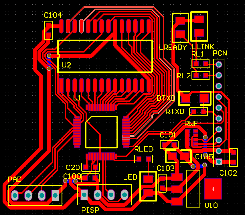
In actual circuit design projects, sometimes it is necessary to adjust the order of leads for convenience in wiring. In complex circuit designs, advantages can be gained by using large-scale programmable logic devices like FPGA or CPLD to adjust the order of external leads of the chip, facilitating wiring. Of course, this also increases design complexity and the additional cost of chips.
Hardware Debugging
1. External RAM Experiment
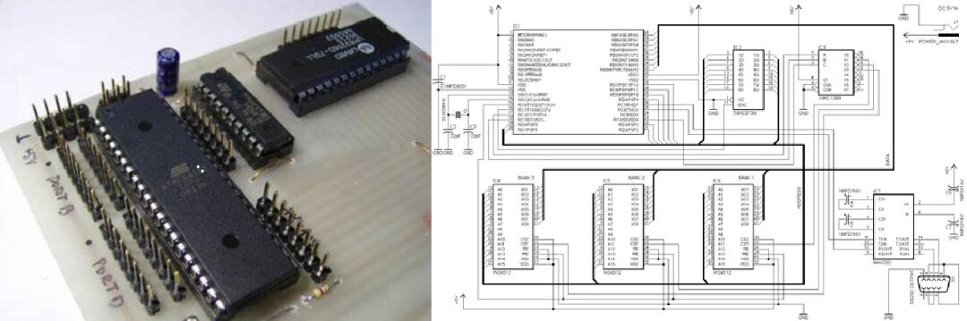
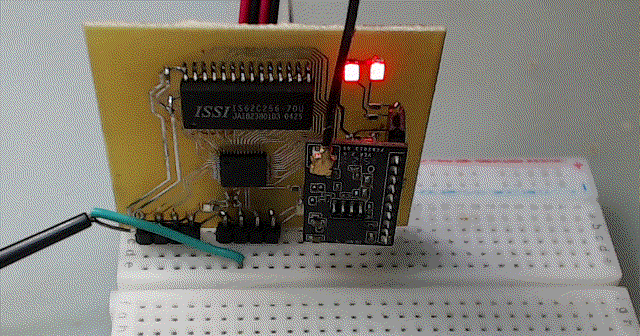
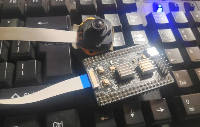
Through design, circuit board corrosion, soldering, and installation, the experimental circuit was quickly obtained.Below is the testing of it.
The hardware programming option configuration for the STC8H microcontroller is as follows:
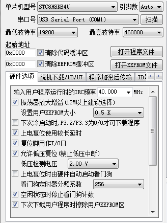
Main indicators of the microcontroller operation:
-
Internal Operating Frequency: 40MHz -
ISP UART1 Baud Rate: 500000bps; -
WiFi-UART Baud Rate: 460800bps
(1) External RAM Access Time Length
Using the MCU’s port to measure the access time to external RAM, the measured time for writing to external RAM is 534ns (including the operation time for FLAG_PIN).
            ON(FLAG_PIN);
            ExtSramWrite(0x0, 0x0);
            OFF(FLAG_PIN);
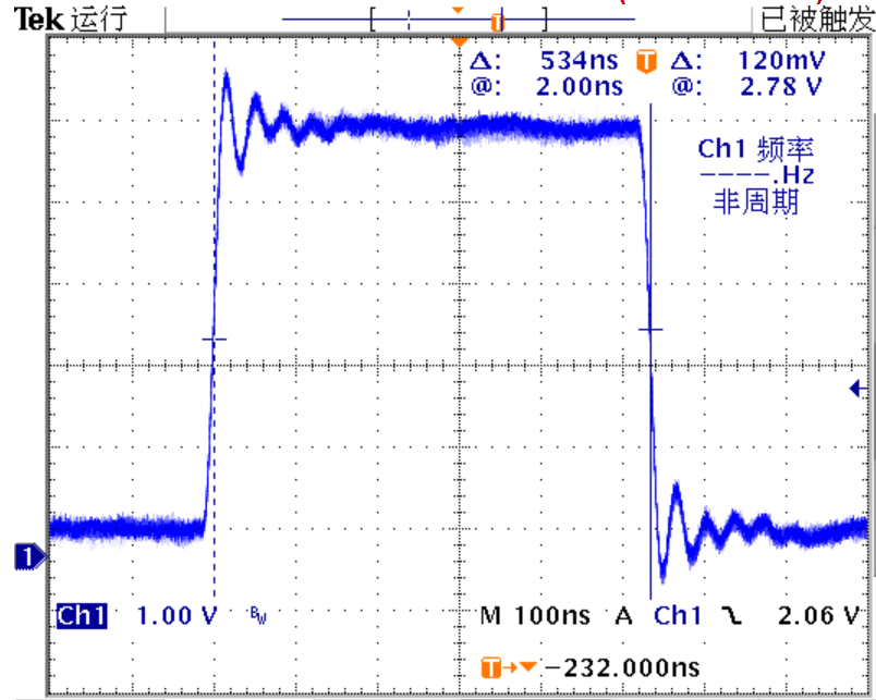
Using the same method, the time for testing ExtRamRead() was found to be 490ns.
2. AD Conversion Experiment
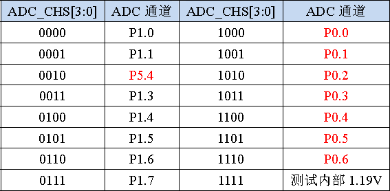
(1) AD Channel Settings:
Using P1.0 and P1.1 to collect two external analog signals.
(2) AD Conversion Time:
-
AD Parameter Setting: STC8H Internal Conversion Start -
AD Conversion Time: Measured by outputting pulses from ADC2 (P1.4). -
Measurement Result: Two ADC conversions took 5 microseconds;
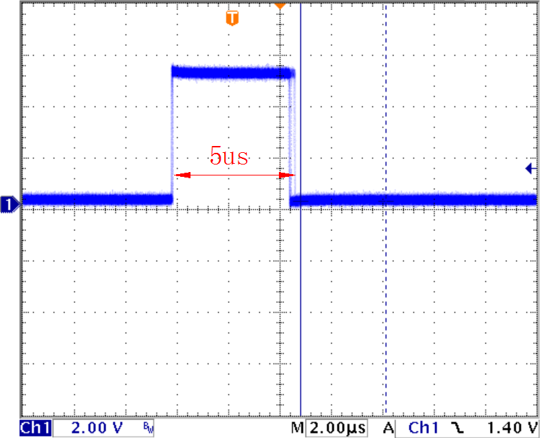
        ON(FLAG_PIN);
        ADCSetChannel(0);
        g_nADResult1 = ADCConvert();
        ADCSetChannel(1);
        g_nADResult2 = ADCConvert();
        OFF(FLAG_PIN);
Collecting Actual Signals
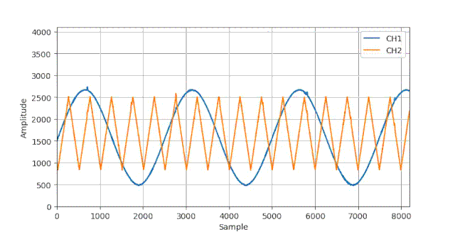
1. Collecting Two Test Signals The following figure shows the waveforms of the collected two test signals:
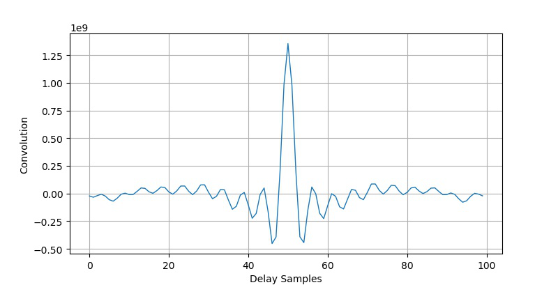
2. Collecting Chirp Audio Signals
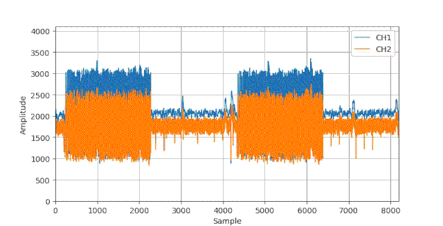
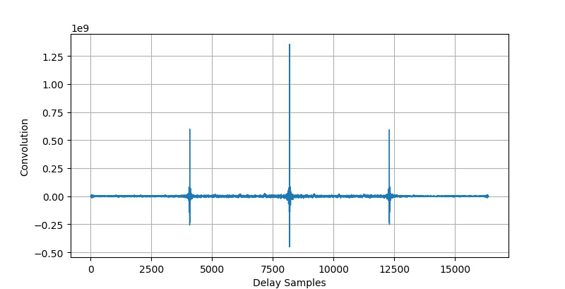
Collecting Chirp signals from both the frequency modulation receiving module and the microphone sensor, and calculating their correlation signals to determine the time delay.
The following figure shows the collected sound signal, which lasts for 0.8192 seconds and contains data for two Chirp signal cycles.
Public Account Message
ZhuoDear, to be honest, this competition was really rushed. The school returned around early June, and then we had to prepare for the final exams. Our team participates in the upright energy-saving group. Other groups might be able to make cars without instruments, but we absolutely cannot. Once there is a problem with the charging board and car model, the correction cycle is calculated in weeks. According to previous seniors’ progress, the normal time left for software debugging before the competition is only about half a month, and now the preparation time has been compressed to two months. This time the software rules are also more difficult than before. It feels like unless we stay up all night every day after school starts, we really cannot ensure the stability of the car.
Please consider the energy-saving brothers.

Reply: Now, I can only say: Brothers, keep it up.
Hello, Teacher Zhuo, sorry to disturb you late at night. Can this chip be used in the beacon group, or does any microprocessor involved in control have to use Infineon?
Reply: This chip can be applied to the beacon group if it is only used for motor drive design and does not participate in other motion control.
Teacher Zhuo, I heard a suggestion that some students discussed in the group about using 1064 to make OpenMV. In fact, secretly using 1064 to run the beacon, although I have not verified its feasibility, I do not want this idea to harm the fairness of the competition, nor do I want to see OpenMV banned as a result, so I mentioned this idea to you.
Another suggestion: The sound beacon competition should only allow the use of finished OpenMV.
Reply: Thank you for reflecting this situation and for your suggestions.
References
Sound Beacon Signal: https://blog.csdn.net/zhuoqingjoking97298/category_9689868.html
[2]High-Speed ADC Collection Board Based on STC8G8K64U: https://zhuoqing.blog.csdn.net/article/details/105731860