Today’s Highlights
1. Three Major Manufacturers Compete for the HBM Market2. Phison Releases Enterprise SSD Controller3. LG Launches HBM Bonding Equipment4. Taiwan Semiconductor Manufacturing Company Revenue to Exceed 100 Billion5. Wafer-Level Packaging Doubles Computing Power
01
Three Major Manufacturers Compete for the HBM Market
Samsung Electronics, SK Hynix, and Micron are expanding their supply of HBM products to ASIC design companies as the demand for custom semiconductors dedicated to AI models from Amazon, Meta, and Google surges, leading to rapid growth in the ASIC market.
The demand for custom semiconductors for AI models has been driven by the high prices and performance efficiency bottlenecks of general-purpose AI chips from NVIDIA and AMD.
Industry experts predict that ASIC shipments will surpass NVIDIA’s AI semiconductor supply next year, with the global AI ASIC market expected to reach approximately $30 billion this year, growing at an annual rate of over 30%, and ASIC shipments are likely to exceed NVIDIA’s AI chip supply.
Currently, the demand for HBM related to ASICs accounts for only about 10% of the total market, concentrated in NVIDIA and AMD, with supply rapidly diversifying.
Companies like Amazon and Google are becoming new powerhouses in HBM procurement with their self-developed ASIC platforms, with Micron clearly identifying ASIC design companies as core customers in its financial report, while SK Hynix has supplied Amazon and Google, and Samsung Electronics will provide HBM3E to Broadcom.
As HBM4 (the sixth generation of HBM) becomes mainstream in 2026, the proportion of HBM procurement by ASIC manufacturers may exceed 30%, shifting the HBM market from being “NVIDIA-dominated” to “diversified competition.”
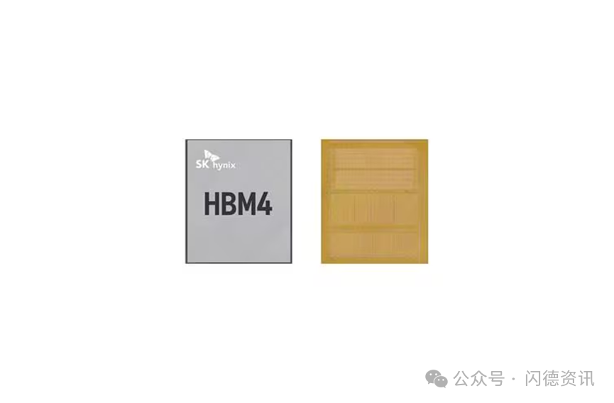
The diversification of the HBM market is a deep transformation of the AI industry from “general computing power” to “customized solutions,” and the deep integration of ASICs and HBM will change the distribution of power in the AI hardware ecosystem, potentially leading to a reconstruction of AI server hardware architecture in the future.
Manufacturers are accelerating capacity layout, with SK Hynix showcasing a 12-layer structure HBM4 that can optimize logic chip designs based on customer needs, significantly improving bandwidth and energy efficiency compared to previous generations. Micron has delivered HBM4 prototypes to customers and started validation, while Samsung plans to invest in HBM4 production line facilities, with all three aiming to seize the opportunity as HBM4 becomes mainstream in 2026.
Analysts point out that if storage manufacturers can establish strategic partnerships with leading ASIC companies in the HBM4 era, they may dominate the future AI storage market.
This change will not only reshape the HBM supply chain but may also compel traditional customers like NVIDIA and AMD to adjust their procurement strategies, intensifying the technological and market competition in the storage chip industry.
02
Phison Releases Enterprise SSD Controller
At the FMW 2025 Global Flash Memory Summit, Phison Technology unveiled the next-generation enterprise SSD controller SM8466 based on the PCIe Gen6 standard.
SM8466 belongs to Phison’s MonTitan enterprise controller family, utilizing TSMC’s 4nm process, compliant with NVMe 2.0+ and OCP NVMe SSD Spec 2.5 standards, equipped with 16 NAND channels, supporting 3D NAND flash types, and capable of achieving a maximum capacity of 512TB with sequential read speeds of 28GB/s and random read/write performance of 7000K IOPS.
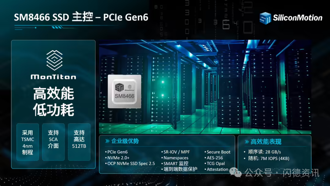
SM8466 supports SCA interface, SR-IOV/MPF virtualization technology, namespaces, S.M.A.R.T parameter monitoring, E2E data protection, Secure Boot, AES-256/TCG Opal encryption, and other features.
While the exact launch date has not been disclosed, the CEO expects shipments of products featuring the SM8466 controller to begin between late 2026 and early 2027, coinciding with the production capacity of NVIDIA’s next-generation AI servers.
Phison believes that AI will be the primary application area for PCIe Gen6 storage, while consumer-grade PCs will not see demand for PCIe 6.0 x4 SSDs until after 2030.
03
LG Launches HBM Bonding Equipment
LG Electronics is fully investing in the development of HBM hybrid bonding machines to align with the group’s AI business strategy and B2B business expansion needs, with its production engineering research institute initiating the development of related equipment, aiming for large-scale production by 2028.
The hybrid bonding machine is used to connect multiple semiconductor chips and, unlike traditional thermocompression bonding technology, can stack chips without bumps, offering advantages such as thinner combined chips and reduced heat generation, which is expected to change the HBM production landscape.
LG Electronics hopes to rapidly expand sales and become a strong competitor in the semiconductor equipment market, with successful development potentially winning over major clients like SK Hynix and enhancing its position in the semiconductor equipment market.
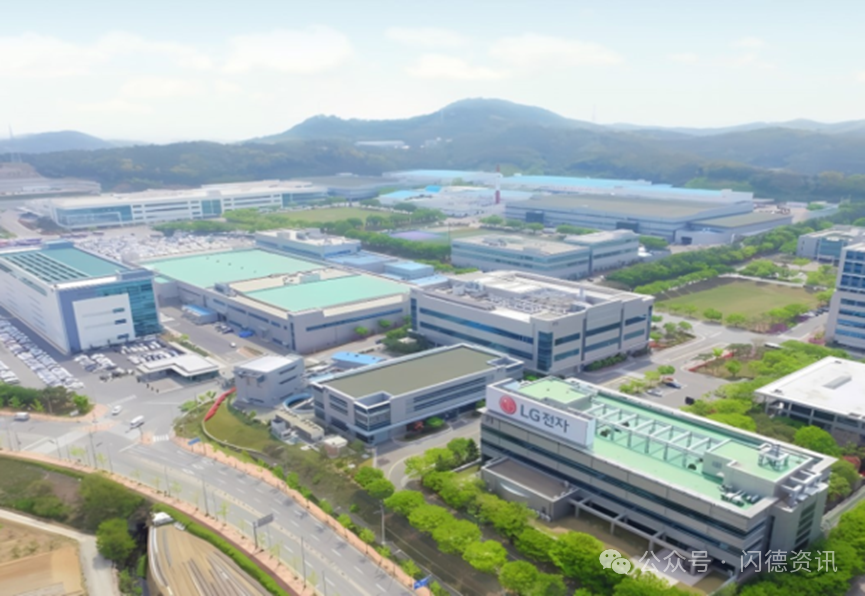
Currently, leading companies in semiconductor hybrid bonding equipment include Dutch company Besi and American company Applied Materials, while South Korean manufacturers SK Hynix and Samsung lead HBM production and show strong interest in localizing equipment.
Samsung Electronics plans to use hybrid bonding machines to produce HBM4 within the year, while SK Hynix will use them for HBM4E, and companies like Hanwha Semiconductor and Hanmi Semiconductor are also actively laying out hybrid bonding machine-related businesses.

04
TSMC Revenue to Exceed 100 Billion
TSMC is optimistic about revenue growth this quarter and for the entire year, driven by the volume production of NVIDIA’s GB300 AI chip and the new iPhone 17 series stock-up, indicating advantages in business with these two key customers, and is expected to achieve excellent revenue results.
Revenue is expected to increase by 3%-7% this quarter, stabilizing above $30 billion, with the possibility of exceeding $100 billion in revenue by 2025.
This Thursday (17th), TSMC will hold a financial briefing to announce last quarter’s and the first half’s financial reports, as well as the outlook for this quarter.
Analysts believe that due to the strong appreciation of the New Taiwan Dollar, last quarter’s financial report may show a decline in profits, with gross margin and operating margin approaching lower limits; however, the volume production of NVIDIA’s GB300 in the second half will drive TSMC’s HPC business, and the launch of NVIDIA’s next-generation AI chip platform Rubin in 2026 will keep TSMC’s 3nm capacity under continuous pressure.
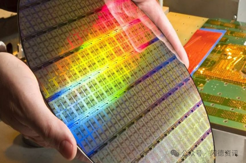
The GB300 chip significantly enhances performance, serving as a key driver for AI inference operations and related applications. NVIDIA continues to outsource production to TSMC, which not only boosts TSMC’s HPC business but also intensifies competition among supply chain players for opportunities in assembling end AI servers, altering the industry landscape.
At the same time, the AI functionality upgrades in Apple’s iPhone 17 series, with silicon content growth outpacing shipment volume, represent TSMC’s largest export market for 3nm, and it will also be the first customer for 2nm capacity, solidifying a long-term partnership that provides strong support for TSMC’s advanced process orders.
05
Wafer-Level Packaging Doubles Computing Power
xAI, owned by Elon Musk, has released the world’s strongest AI model, Grok 4, with the Dojo system being the biggest contributor, thanks to TSMC’s System on Wafer (SoW) packaging technology.
This technology treats the wafer as a complete system, facilitating Tesla’s goals through precise wafer-level interconnections and integrations, with industry analysts estimating that the computing power is at least five times that of CoWoS, and the market is optimistic about TSMC maintaining its technological lead in advanced packaging.
As the parameters of AI large models grow rapidly, the demand for computing power has surged a thousandfold in two years. Single-chip GPUs are approaching their limits due to physical size constraints, and multi-chip interconnections face data latency and loss issues.
The Dojo system adopts a Chiplet approach, integrating 25 D1 chips on a wafer-sized substrate, created using TSMC’s InFO-SoW technology, with mass production of the AI supercomputer Dojo 2 system expected by the end of the year.
SoW, as a wafer-level packaging technology, achieves high-density interconnections through 3D stacking and re-routing layers, and the demand for advanced packaging capacity is expected to increase significantly in the future. SoW-X is expected to be ready by 2027, integrating various components to create a powerful wafer-level system.
Analysts believe that SoW-X can be seen as a large module package, packaging 16 ASICs and dozens of HBM chips on a single wafer, making yield control the biggest challenge, with the 9-fold mask size posing new design challenges for heat dissipation, such as introducing liquid cooling and immersion cooling. Companies like ChipMOS and Unimicron are expected to benefit.
SoW is TSMC’s disruptive packaging technology developed to meet the endless demands for computing power, memory bandwidth, and integration from future AI and HPC applications, realizing the vision of “a complete wafer as a super system.”
END

Resource Center