Below, we analyze the working principle of the smartphone camera circuit using the Huawei Nova 5 as an example. The Nova 5 is equipped with a 48-megapixel AI quad-camera setup, which includes wide-angle, telephoto, macro, and depth cameras, capable of meeting all-day photography needs; it also features a 32-megapixel front camera.
1. Front Camera
The front camera, also known as the secondary camera, is located above the phone screen. The Nova 5 uses a 32-megapixel camera. The front camera can be used for selfies, video calls, and more.
The front camera circuit is shown in Figure 1.
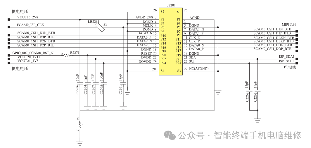
Figure 1: Front Camera Circuit
The power supply voltage VOUT13_2V8 is sent to pin 2 of J2201; the power supply voltage VOUT20_1V11 is sent to pin 22 of J2201; the power supply voltage VOUT21_1V8 is sent to pin 24 of J2201.
The clock signal FCAM0_ISP_CLK1 is sent to pin 6 of J2201; the reset signal GPIO_007_SCAM0_RST_N is sent to pin 20 of J2201; the I2C bus is sent to pins 21 and 23 of J2201.
The front camera communicates with the application processor via the MIPI bus.
2. Main Rear Camera
The main rear camera generally refers to the camera located on the back of the phone. The main camera has a higher pixel count than other cameras and offers more features, assisting the phone in completing primary photography tasks.
The main rear camera circuit is shown in Figure 2.
The main rear camera has multiple power supply voltages, namely VOUT25_2V85, VOUT4_1V8, VOUT20_1V11, VOUT21_1V8, and VOUT19_2V8, which provide power to the camera.
The reset signal GPIO_008_MCAM0_RST_N is sent to pin 28 of J2301, and the reset signal RCAM0_ISP_CLK0 is sent to pin 6 of J2301.
The main rear camera communicates with the application processor via the MIPI bus.
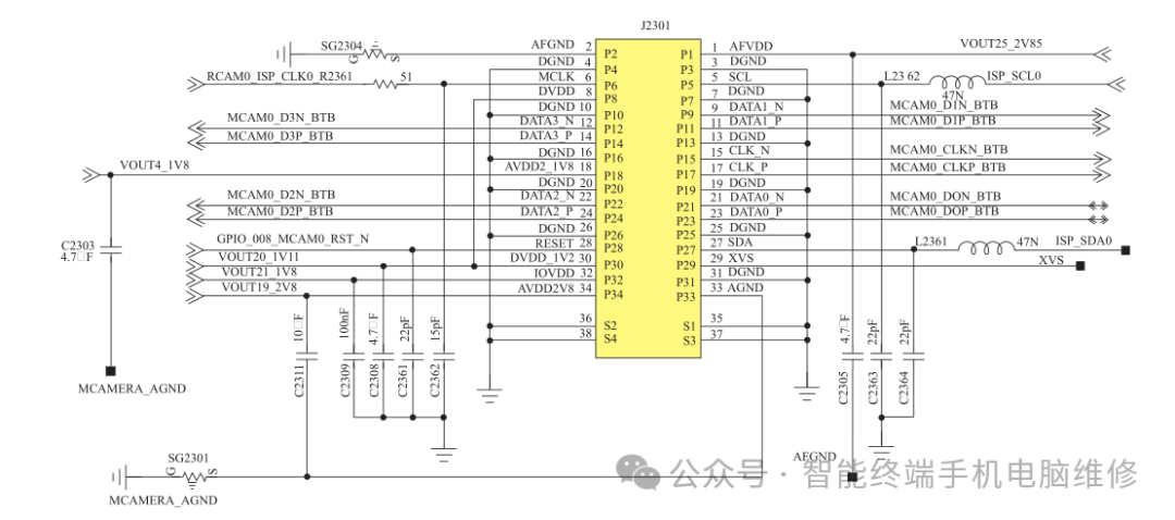
Figure 2: Main Rear Camera Circuit
3. Wide-Angle Camera
The wide-angle camera generally refers to a camera with a field of view greater than 120°. The lens of a wide-angle digital camera has a short focal length, providing a wide angle and a deep depth of field, making it suitable for capturing larger scenes such as architecture and landscapes.
The wide-angle camera circuit is shown in Figure 3.
The power supply voltage VOUT22_2V8 is sent to pin 1 of J2302, the power supply voltage VOUT32_1V11 is sent to pin 21 of J2302, and the power supply voltage VOUT21_1V8 is sent to pin 23 of J2302.
The reset signal GPIO_010_MCAM1_RST_N is sent to pin 19 of J2302, the clock signal RCAM1_ISP_CLK2 is sent to pin 5 of J2302, and the I2C bus signals are sent to pins 22 and 24 of J2302.
The wide-angle camera communicates with the application processor via the MIPI bus.
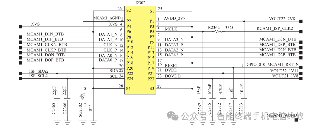
Figure 3: Wide-Angle Camera Circuit
4. Macro Camera
The macro camera is a special lens used for macro photography, primarily for capturing very small objects such as flowers and insects. To focus correctly on subjects that are very close, macro cameras are typically designed to extend longer, allowing the optical center to be as far from the photosensitive element as possible. Additionally, the lens group design must focus on controlling distortion and chromatic aberration at close distances.
The macro camera circuit is shown in Figure 4.
The power supply voltage VOUT13_2V8 is sent to pin 3 of J2303, the power supply voltage VOUT21_1V8 is sent to pin 5 of J2303; the reset signal GPIO_012_MCAM2_RST_N is sent to pin 9 of J2303, the clock signal RCAM1_ISP_CLK2 is sent to pin 2 of J2303, and the enable signal GPIO_219_MCAM2_VCM_PWDN is sent to pin 11 of J2303.
The macro camera communicates with the application processor via the MIPI bus.
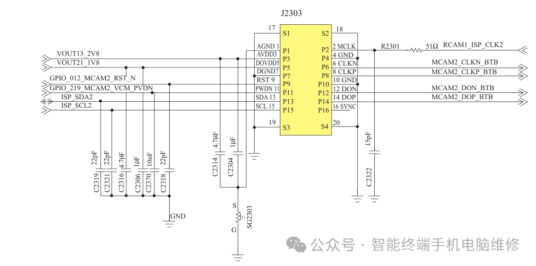
Figure 4: Macro Camera Circuit
5. Depth Camera
The depth camera is used to calculate the depth of the subject (mainly people) and does not directly participate in imaging. The depth camera can detect the distance of objects, which is beneficial for blurring the background and highlighting the subject. With the same aperture and distance, a shorter focal length results in a greater depth of field.
The depth camera circuit is shown in Figure 5.
The power supply voltage VOUT13_2V8 is sent to pin 3 of J2303, the power supply voltage VOUT21_1V8 is sent to pin 5 of J2303, the reset signal GPIO_012_MCAM2_RST_N is sent to pin 9 of J2303, and the clock signal RCAM1_ISP_CLK2 is sent to pin 2 of J2303.
The depth camera communicates with the application processor via the MIPI bus.
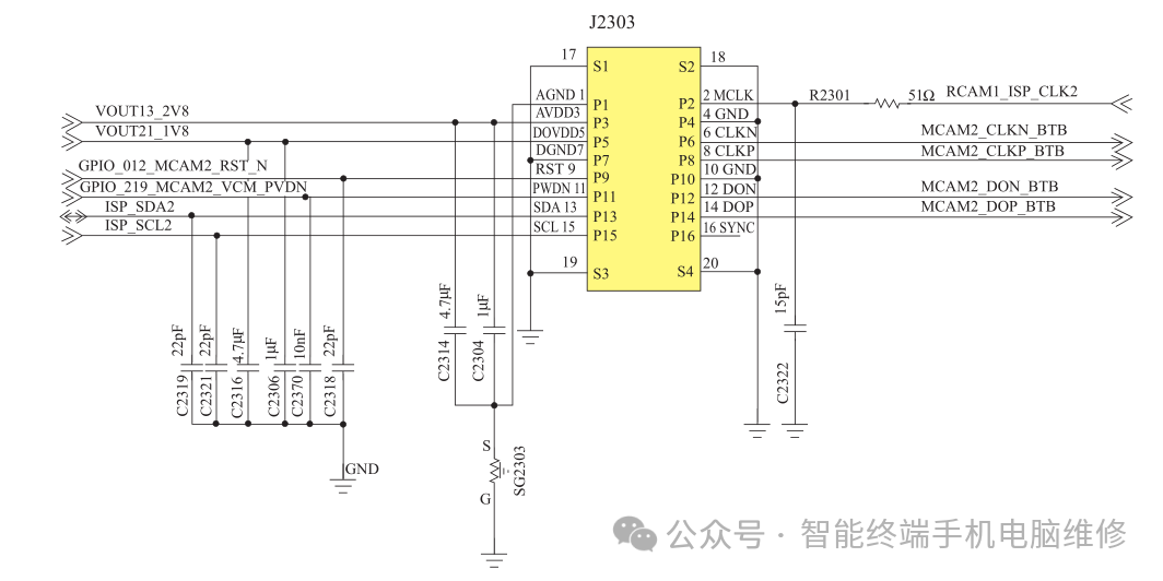
Figure 5: Depth Camera Circuit
6. MIPI Bus Electronic Switch
To better utilize resources, an electronic switch for the MIPI bus is also used in the smartphone camera circuit, facilitating the switching between the wide-angle lens, depth lens, and macro lens.
The MIPI bus electronic switch is shown in Figure 6.
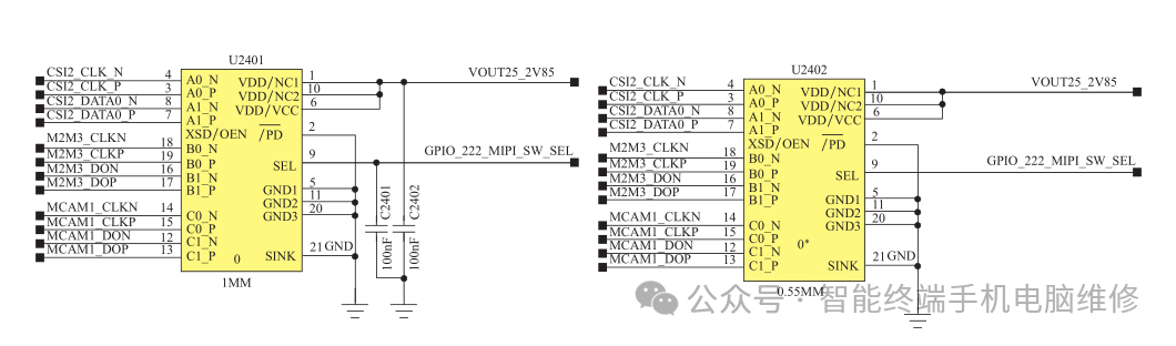
Figure 6: MIPI Bus Electronic Switch
7. Flash Circuit
The monochrome flash is simply a white LED flash, which has limited brightness and range, while the dual-color temperature flash consists of two LEDs (orange + white), providing stronger brightness and a wider range.
The dual-color temperature flash produces softer imaging effects compared to the monochrome LED flash, and the white balance is more accurate, which significantly improves photo quality in low-light conditions.
Currently, most smartphones on the market use a high-brightness WLED (white light-emitting diode) flash combined with a slightly dimmer amber LED warm light to achieve color temperature compensation.
The flash circuit is shown in Figure 7.
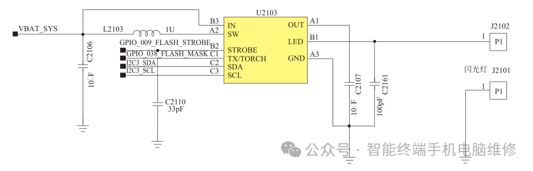
Figure 7: Flash Circuit
The power supply voltage VBAT_SYS is sent to pin B3 of the flash chip U2103; the I2C bus signals are sent to pins C2 and C3 of U2103; the flash control signal GPIO_009_FLASH_STROBE is sent to pin B2 of U2103; the mode control signal GPIO_038_FLASH_MASK is sent to pin C1 of U2103, controlling the operation of U2103.
The flash signal is output from pin B1 of U2103, driving the LED flash.