Life does not have the best solution; we can have multiple ways of living and refuse to limit ourselves. Joining this knowledge community can expand your network, break your cognitive boundaries, and connect you to over 40,000 insiders in the automotive industry, exchanging career information, bridging workplace information gaps, meeting peers, and exploring technical communication and career development together.
The discussion about Tesla’s autonomous driving technology is very lively in the industry. Tesla’s vision-based approach, while advantageous from a cost perspective, has the most complex algorithms and control systems. In contrast, another leader in the autonomous driving field, Waymo, insists on a lidar-first technology route, which is relatively easier to implement, but the high cost of lidar poses obstacles to mass production. However, in the domestic autonomous driving industry, lidar is generally used in levels above L3, with multiple examples such as Baidu Apollo and Pony.ai. Recently, I have been following the online disassembly of Tesla’s Autopilot AP3.0, and as a somewhat unconventional engineer in the industry, I decided to take some notes.
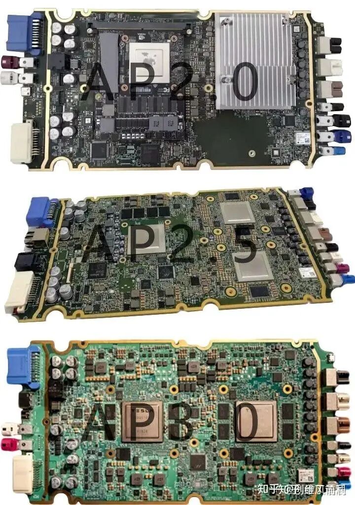
Comparison of Tesla AP2.0, AP2.5, and AP3.0 Circuit Boards
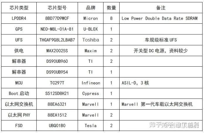
According to estimates from Zosi Automotive Research, the price of a single computing chip is approximately 5000 RMB, and the cost of the entire board is around 7500-8500 RMB (including connectors). Although automotive-grade connectors, especially high-speed Ethernet connectors, are relatively expensive, we cannot overlook the cost of this PCB, which is produced by TTM in the USA and can compete with computer motherboards, with a mass production price estimated to be around 200 RMB. The optional price for Tesla’s FSD is 56,000 RMB. Although there is a software cost allocation, this price is indeed a bit steep. It is said that this AP3.0 is also manufactured by Quanta Computer (the world’s largest notebook computer OEM) at its factory in Songjiang, Shanghai. LPDDR stands for Low Power Double Data Rate SDRAM, a type of DDR SDRAM, also known as mDDR (Mobile DDR SDRAM), which is currently the most widely used “working memory” in mobile devices worldwide. Tesla’s LPDDR4 (8BD77D9WCF) is supplied by Micron. The 8 indicates the year 2018, B indicates the 4th week, D represents D-Die, which belongs to Micron’s product line with relatively average performance. The 77 indicates the chip’s production and packaging location, with 7 representing Taiwan (5 representing mainland China). Therefore, this is a D-Die particle produced by Micron in the second week of 2018. The D9WCF corresponds to the model MT53D512M32D2DS-046AAT. 53 indicates that this is an LPDDR4 particle; D indicates a working voltage of 1.1V; 512M indicates that the capacity of a single particle is 512MB; 32 indicates that the single particle width is 32bit; D2 indicates that this particle is a dual-layer package, meaning that there are two 512MB particles in a single package, with a total capacity of 1GB; DS is the packaging number; 046 indicates that the working frequency of this particle is 2133MHZ; the first A indicates Automotive, meaning it is an automotive-grade particle; the following AT indicates Automotive Temperature. The GPS module for FSD is NEO-M8L-01A-81, with a horizontal accuracy circular error probable (CEP) of 2.5 meters, which can be reduced to 1.5 meters with SBAS assistance, receiving GPS/QZSS/GLONASS/BeiDou. CEP and RMS are units of GPS positioning accuracy (commonly referred to as precision), which are units of error probability. Cold start takes 26 seconds, hot start takes 1 second, and assisted start takes 3 seconds. It has a built-in simple 6-axis IMU with a refresh rate of 20Hz, and if produced in large quantities, the price will be below 300 RMB. UFS (Universal Flash Storage) uses THGAF9G8L2LBAB7, a new product mass-produced by Toshiba in mid-2018, meeting automotive-grade UFS standards, AEC-Q100 Level 2, with a capacity of 32GB. Since Tesla’s algorithm model does not occupy much space, it is sufficient. MAX20025S is a switching power supply regulator that provides power to the memory, sourced from Maxim Integrated, and currently, more introduction materials cannot be found. S512SD8H21 is likely the Boot startup chip supplied by Cypress (which has been acquired by Infineon). On the right side of the Tesla board, from top to bottom, are the FOV camera, fisheye surround camera, left and right A-pillar cameras, left and right B-pillar cameras, front main camera, in-cabin DMS camera, rear camera, and GPS coaxial antenna. On the left side, from top to bottom, are the second power supply and I/O interfaces (body LIN network, etc.), Ethernet diagnostic in/out, debugging USB, programming, main power supply, and I/O (chassis CAN network, etc.). Tesla uses three TI FPD-LINK chips, which are deserializer chips. Deserializer chips are used in pairs, with the serializer generally inside the camera and the deserializer on the PCB. Two DS90UB960 chips correspond to DS90UB953-Q1, DS90UB935-Q1, DS90UB933-Q1, and DS90UB913A-Q1. The DS90UB960 has 4 lanes, and if it is a MIPI CSI-2 port, the bandwidth for each lane can be set between 400Mbps and 1.6Gbps.
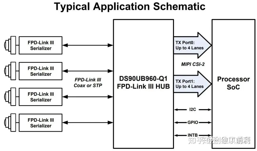
The above image is a typical application diagram recommended by TI for the DS90UB960, which connects 4 2MP cameras at a frame rate of 30Hz with YUV444 data, or 4 2MP cameras at a frame rate of 60Hz with YUV420 data. The DS90UB954 is a simplified version of the DS90UB960, reducing from 4 lanes to 2 lanes, and is used in conjunction with the DS90UB953. Since most cameras’ LVDS format can only be used for short-distance transmission, each camera must be equipped with a deserializer chip to convert parallel data into serial for transmission via coaxial or STP, allowing for longer transmission distances and easier compliance with automotive EMI standards. Currently, the most commonly used deserializer chips in the industry are from Texas Instruments (TI) and Maxim, with Tesla using TI, while we often encounter Maxim in development, possibly due to NVIDIA’s AI chip platform design recommendations. Most cameras used in intelligent driving are based on Maxim solutions.(Camera data formats typically include RAWRGB and YUV. Common YUV formats include YUV444, YUV422, and YUV420. The formula for calculating bandwidth is pixels * frame rate * bits * X. For RAW RGB, X=4. For example, if a camera outputs 30Hz at 2MP, the bandwidth is 2 million x 30 x 8 x 4, which equals 1.92Gbps. YUV444 is pixels x frame rate x bits x 3, which equals 1.44Gbps; YUV422 is pixels x frame rate x bits x 2, which equals 0.96Gbps; YUV420 is pixels x frame rate x bits x 1.5, which equals 0.72Gbps. ADAS generally does not consider color much, so YUV420 is sufficient. Besides automotive applications, YUV422 is often used.)
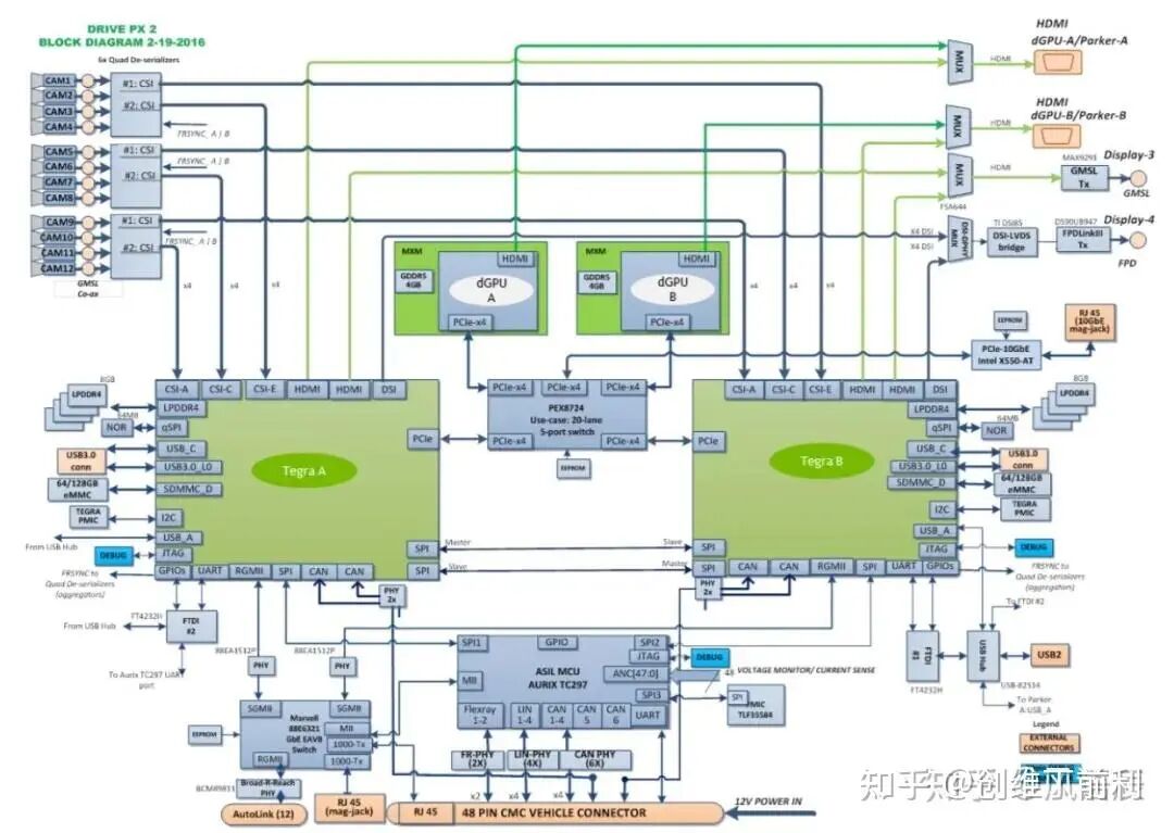
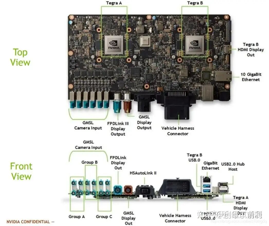
The above image shows the NVIDIA Drive PX2 framework diagram and interface schematic, indicating the use of 12 GMSL interfaces. NVIDIA uses Maxim’s GMSL for deserialization. Clearly, NVIDIA uses three Maxim GMSL chips, each connected to 4 cameras (there are rumors that Maxim may have custom-made GMSL deserializer chips for NVIDIA). Currently, Maxim’s highest-level GMSL chip is MAX9296, with the corresponding chip in the camera being MAX9295, with a maximum bandwidth of 12GBps, capable of supporting two 8MP cameras. This combination is currently the highest configuration in the industry, and apart from some large companies or Tier 1 suppliers, other R&D companies generally cannot access it. Among TI’s mass-produced chips, the highest is DS90UB960, which can only support a bandwidth of 6Gbps. Currently, the application of GMSL combined with MIPI CSI-2 for high-pixel ADAS applications is mainstream, although some recommend higher-performance Ethernet, but currently, automotive Ethernet is still immature and mostly used for lidar. The competition between MIPI (LVDS, MIPI is a type of LVDS protocol) and Ethernet is currently lagging behind for Ethernet. Compared to LVDS, Ethernet has advantages such as higher bandwidth, stronger reliability, comprehensive link layer protocols, better security, lower latency, and more flexible bus topology, making it easier to bridge and switch.
However, for the automotive industry, although automotive Ethernet has been quite popular in recent years, it is still a relatively new concept and has not yet formed a unified standard. R&D engineers need time to explore and familiarize themselves, while MIPI is already very mature and almost monopolizes the automotive camera market, making it much easier for engineers to apply, resulting in shorter development cycles. Currently, the Ethernet camp includes Marvell, Broadcom, Renesas, NXP, and most traditional network communication manufacturers. On the LVDS side, only Texas Instruments and Maxim are capable of handling deserialization. There are very few PHY manufacturers that can provide over 10Gbps bandwidth in the Ethernet field, with Aquantia being the most common, but it was acquired by Marvell in May 2019 for $452 million. Aquantia is known for its 10G network cards, which reportedly cost $130 each. Recently, I have been researching PHY switches, and the lack of resources in the industry, coupled with the high prices, is indeed frustrating! The MCU is Infineon TC297T, which is currently the only choice and is widely used in the industry, such as in ZF’s domain controller or other domain controllers based on Xavier design. FSD does not use PCIe Ethernet switches, and as an SoC chip, it does not integrate PHY chip functions. It is estimated that, like AP2.5, it still uses 88EA1512. Tesla uses 88EA6321 to connect two FSDs as the core for data exchange, which may also include GPS and Ethernet diagnostics. Since Tesla does not use lidar, and the millimeter-wave radar uses Bosch’s CAN communication, Ethernet is not involved, which aligns with Tesla’s vision-based approach. The 88EA6321 is Marvell’s first-generation automotive Ethernet switch, providing 7-channel gigabit Ethernet, fully compliant with the IEEE802.3 automotive standard, supporting AVB (Audio/Video Bridging) functionality, and low power consumption.
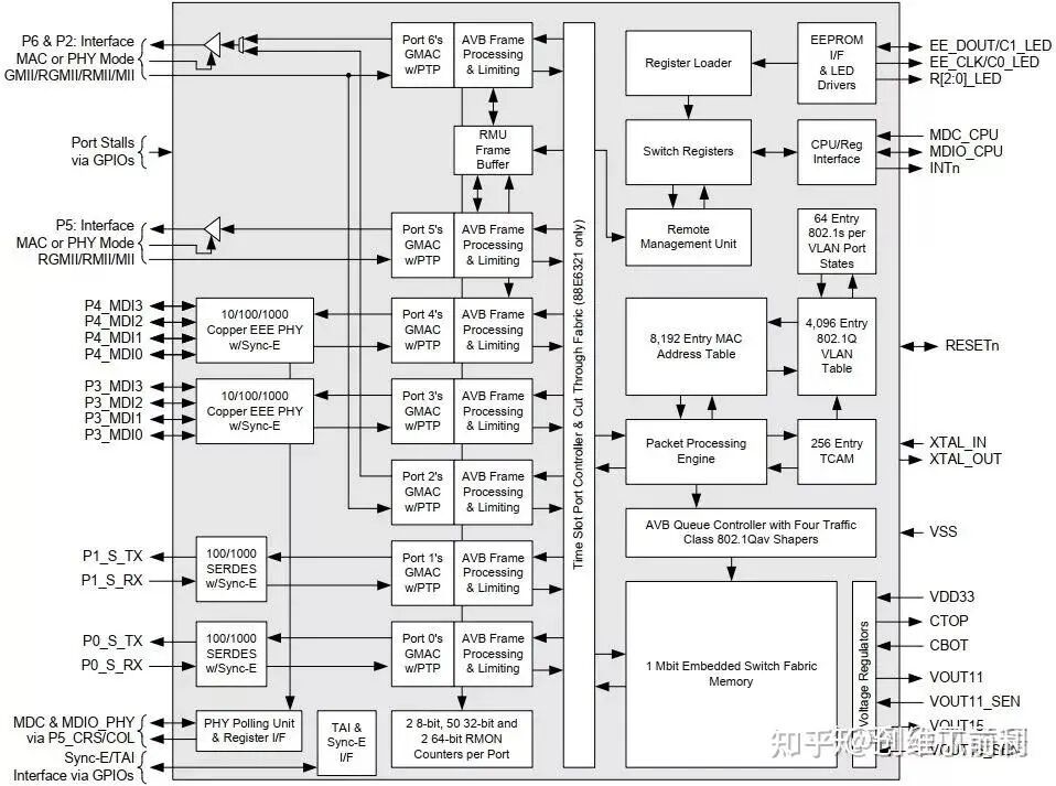
The above image is the internal framework diagram of the 88E6321, which is a 7-port Ethernet switch designed for automotive EAVB, launched at the end of 2014. It has two IEEE 10/100/1000BASE-T/TX/T interfaces (corresponding to the traditional RJ45, commonly known as crystal heads), two RGMII/xMII interfaces or one GMII interface, two SGMII/Serdes interfaces, and one RGMII/xMII interface. MII stands for Media Independent Interface, RMII stands for Reduced MII, SMII stands for Serial MII, and GMII stands for Giga MII. MII is the standard interface connecting MAC and PHY, defined by the IEEE-802.3 Ethernet industry standard. 10/100/1000BASE-T/TX/T refers to transmission cables. Ports 2, 5, and 6 can be configured for MAC mode or PHY mode, supporting RGMII/RMII/MII, and Ports 2 and 6 also support GMII. Ports 3 and 4 support 10, 100, and 1000M adaptive Ethernet interfaces. Ports 0 and 1 support 100M and 1000M optical ports (SFP). Many domestic companies use the 88E6321 for switches, and Bosch has also used it for gateways.
However, EAVB (Ethernet Audio Video Bridging) is not strictly an automotive Ethernet standard; it is a set of transmission protocols for in-vehicle real-time audio and video established by the IEEE 802.1 task group starting in 2005. EAVB has not been widely promoted, as the most typical application for transmitting audio and video streams in vehicles is entertainment systems, which do not need to consider latency. Most other automotive applications are pure video streams, and EAVB requires hardware compression and then decompression, which significantly increases costs. Pure video can use low-cost transmission methods such as GMSL, MIPI, or FPDLINK. In November 2012, the IEEE renamed the EAVB group to TSN (Time Sensitive Networking), which signifies the emergence of a strict automotive Ethernet standard. Of course, TSN is a series of standards. The core advantage of TSN over EAVB is its support for L4, specifically the 802.1CB protocol. This is also the main reason why L4-level autonomous driving must use TSN, as only TSN can enable the entire system to achieve the highest functional safety level, ASIL D. Similarly, it is highly integrated with adaptive AUTOSAR. Additionally, compared to traditional IP/VLAN routing, TSN has several advantages: no CPU processing power and bandwidth bottleneck limitations, no cross-dependencies with other ECUs, faster parallel startup, independent reboot for switches and MCUs, and high flexibility. Tesla’s two FSDs enhance computing power rather than serving as a redundant system. From a safety perspective, L4-level autonomous driving requires a redundant processor, and the role of 802.1CB is to establish a communication mechanism between the main processing system and the redundant processing system. 802.1CB is for redundancy between two systems, while redundancy between chips often uses PCIe switches with multi-host fail-operational mechanisms. Tesla’s switch ports have been reserved, possibly for future expansion considerations, such as V2X. Tesla’s design for FSD is somewhat aggressive in adopting EAVB as the core switch for autonomous driving. Although EAVB is not a standard automotive-grade solution, Tesla’s boldness in the absence of better options is what makes it advanced.