Recently, discussions about Tesla’s AMD vehicle chips have been exceptionally lively. Is AMD really that good? AMD is eternal? Is this a benefit for the party? With the official delivery of the domestic Model Y Performance, the multimedia control unit MCU 3.0 (Media Control Unit) equipped with the AMD main control scheme has officially kicked off its delivery in China.
The first model to feature the AMD platform is the Model S Plaid, which was officially delivered in the North American market in June 2021. The official website shows that the delivery time for the Model S Plaid in China is the end of 2022. Currently, the models equipped with the AMD infotainment system are Model 3/Y, and there are reports that the Model 3/Y delivered in 2022 will gradually switch as well, it’s just a matter of time.
For learning purposes, this article organizes some teardown information of Tesla’s MCU 3.0 and shares it for discussion. The images of the Model S Plaid’s vehicle machine primarily come from Ingineerix’s teardown video, while the teardown images of the Model Y Performance mainly come from “Super Workshop” teardown [1].
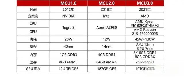
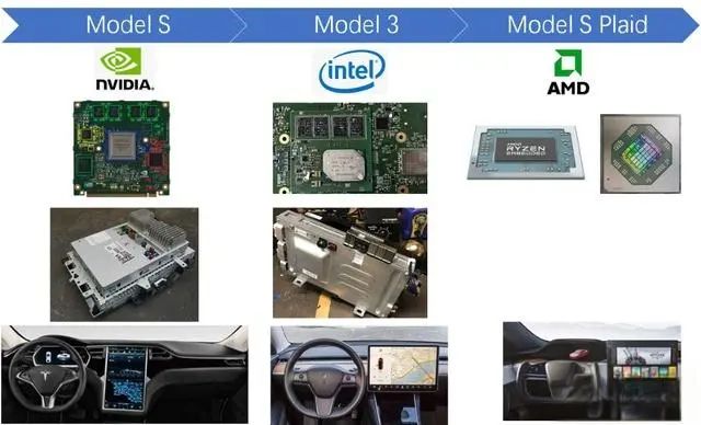
MCU 3.0 is Tesla’s third-generation infotainment system. The MCU 1.0 main control uses NVIDIA’s Tegra 3, while MCU 2.0 uses Intel’s Atom 3950, nicknamed “Atom” in the industry, which is also the main configuration at present. The MCU 3.0 main control has been upgraded to the Ryzen embedded APU and RDNA 2 architecture GPU, and the comparison of the three generations of MCUs is as follows [2].
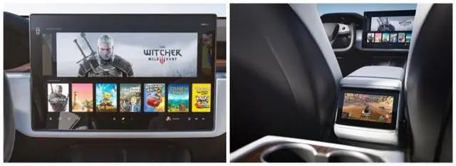
At first glance, MCU 3.0 seems to have moved a desktop workstation into the car. The AMD Ryzen Embedded APU, paired with the AMD RDNA 2 architecture GPU, has an external 8GB GDDR6 graphics card, is internet-connected, supports BT & WiFi, runs a Linux operating system, and supports AAA games, with the ability to connect game controllers. Although there is no keyboard and mouse, the in-car touchscreen is clearly more convenient, and the horizontally arranged large screen enhances the movie and gaming experience.
Currently, the Model S Plaid features 8GB LPDDR4 + 256 SSD + 17-inch touchscreen, while the Model Y Performance has 16GB LPDDR4 + 256 SSD + 15-inch touchscreen.
If we compare MCU 3.0 to a workstation, the previous generation MCU 2.0 resembles a 15-inch tablet or entry-level laptop, with Intel Atom A3950, a clock speed of 1.6GHz, and 4GB DDR4 memory, appearing somewhat ordinary in comparison.
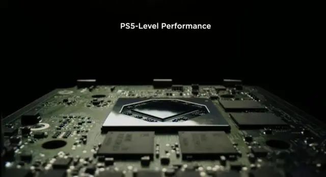
MCU 3.0 brings desktop computing power into the car, and stronger computing power will provide a smoother control experience. It also brings a “PS5” into the car, effectively giving a gaming console with the purchase of the car, capable of running large games like Cyberpunk 2077 and The Witcher, adding more playability and entertainment to the vehicle.
Although gaming is a niche market, and regardless of how many people will actually play AAA games in the car, the hardware performance is genuinely top-notch, leaving plenty of capacity for the vehicle’s applications.
It is evident that maximizing the computing power of the vehicle’s system for a niche market is not cost-effective, but this approach is quite cool, very geeky, and has a high profile, providing users with more unexpected experiences. Users saying “AMD is great” may bring greater value than the money saved.
Tesla is taking a different path from the mainstream domestic approach of [ARM architecture chips + Android systems], opting for [X86 architecture chips + Linux systems]. The former mainly uses mobile solutions, with mainstream chips like Qualcomm’s 8155/8295, while the latter primarily uses PC solutions, with mainstream chips being Intel and AMD.
The advantage of X86 lies in running large software, with Tesla being a typical representative. The vehicle’s operation is based on secondary development of Linux, with a very simple system and good optimized control. Its advantage is the ability to run large games, but its relative disadvantage compared to Android is in the ecosystem; applications like Bilibili and iQIYI in the cockpit are usually web-based, leading to slightly longer loading times.
The advantage of ARM lies in the mature ecosystem of the current mobile internet. The mainstream domestic car companies choose to conduct secondary development based on the Android system, then adapt APP and UI, leading to a superior ecological experience with Android.
Both architectures have their advantages, and the main experience will still depend on the hardware performance and software optimization level of each company. In the PC era, X86 architecture ruled, while in the mobile internet era, ARM has a slight edge. So in the upcoming vehicle applications, which side do you favor?
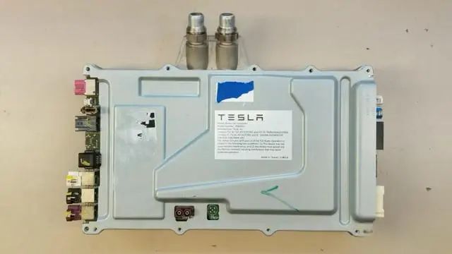
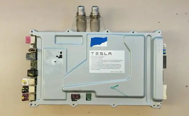
Unlike the previous generation Model S, MCU 3.0 has been placed in the CCM (Central Control Module). The CCM controller’s surface nameplate includes module name, manufacturer, precautions, and other information, with the manufacturing location being Taiwan, China.
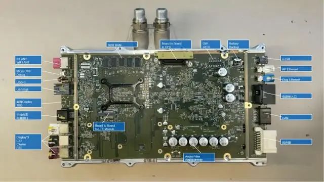
The new CCM has a total of four PCB boards, one more than the Model 3, including 1 multimedia control motherboard, 2 communication small boards, 3 GPU core boards, and another side is 4 autopilot unit boards.
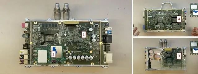
Tesla’s hardware platform is truly excellent, with different PCB boards that can be combined. The communication small boards of Model Y and Model S look exactly the same, and the Autopilot and Model 3 AP 3.0 have basically not changed.
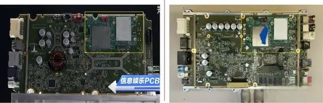
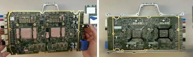
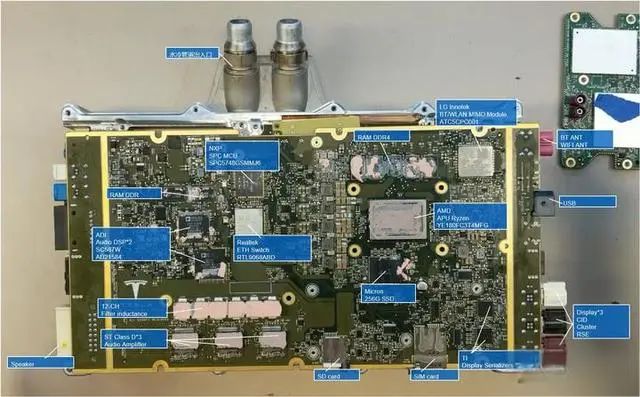
Let’s take a closer look at the significant changes in the two PCBA boards of MCU 3.0. The front side of the large PCBA mainly includes key components such as APU, MCU, ADSP, BT & WiFi modules, display serializers, amplifiers, etc. Key components placed on one side help with the secondary reflow of PCBA production.
The back of the large PCBA mainly prevents some passive components such as resistors and capacitors.
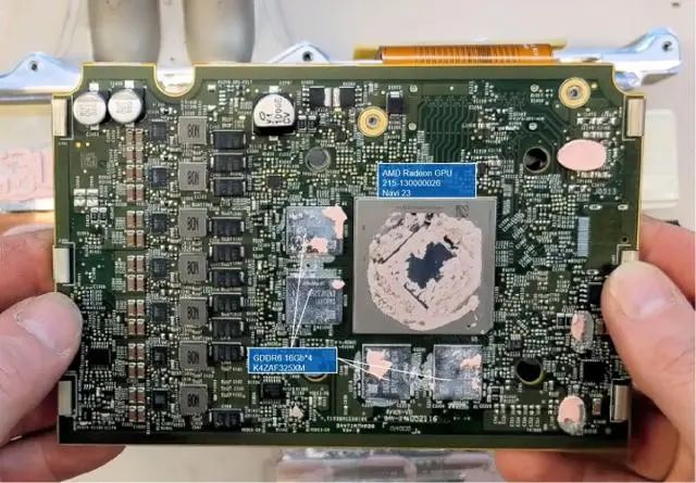
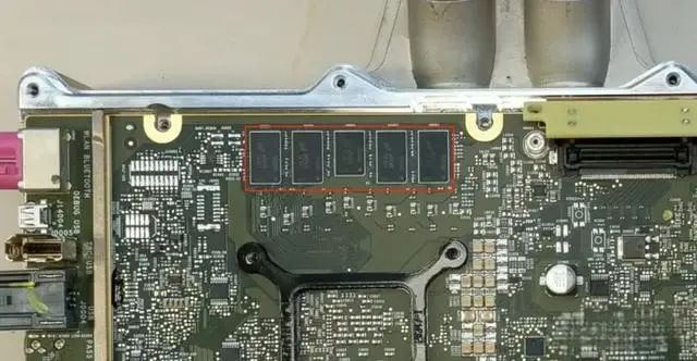
The GPU motherboard mainly consists of the GPU and 4 pieces of GDDR6 dedicated memory, with the GPU’s OPN number being 215-130000026.
The list of key components for MCU is as follows:
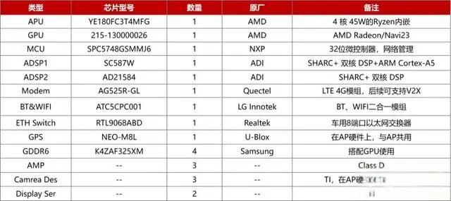
The APU chooses AMD’s Ryzen Embedded V1000 series processor, with the OPN model being “YE180FC3T4MFG”. The official website did not find this APU chip, which should belong to custom materials, conforming to AEC-Q100 automotive certification. APU stands for “Accelerated Processing Units”, which integrates CPU and GPU cores on a single chip.
The material OPN only differs by two letters from V1807B’s “YE1807C3T4MFB” and should belong to the same series, with a base frequency of 3.35GHz (3.8GHz max), 4 cores, and Vega 11 integrated graphics (1300MHz), supporting 2x10Gb Ethernet and a maximum video display capability of 4xHDMI 2.0 or 4xDP 1.4, supporting Dual Channel DDR (memory modules).
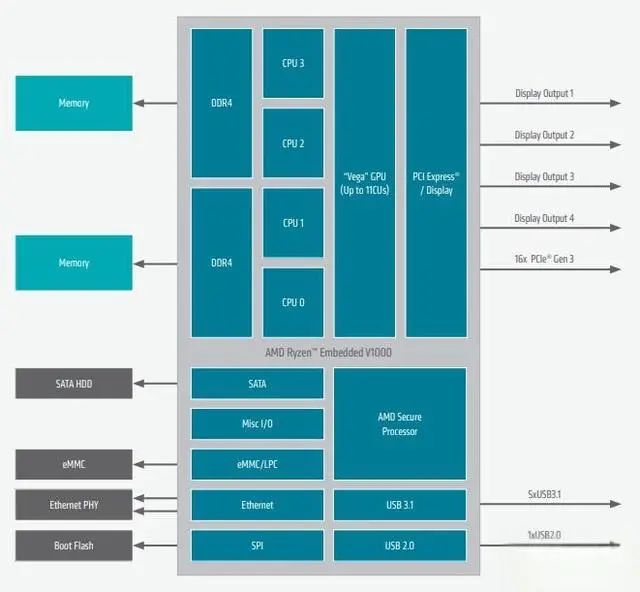
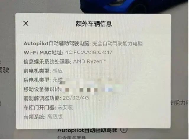
AMD’s official website shows that this APU single SOC can drive the vehicle’s main unit, dashboard, and other display devices, meaning the Model S’s dashboard, central control, and rear screen, while the hardware design has reserved space for a front passenger screen, which may be added later. However, the Model Y P may have only one central control display of 15 inches due to cost considerations.
The APU hard drive is a 256GB SSD, and the DDR memory consists of 10 chips arranged on both sides, with two different silk prints, 8 pieces being D9XSM and 2 pieces being D9XSP.
On Micron’s official website, these two memory models can be found as MT40A512M16LY-062EAAT:E (8Gb=1GB) and MT40A1G8SA-062EAAT:E (8Gb=1GB), with AAT indicating automotive grade, temperature range -40-105℃. D9XSM is x16, with 4 pieces forming x64, and the eight pieces on both sides forming 2 DIMMs (2 memory modules) for a total of 8GB memory.
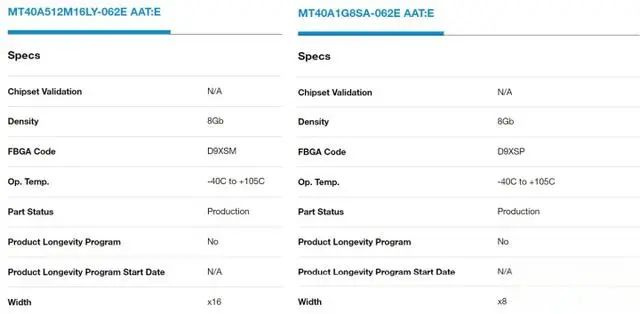
The two D9XSP pieces are x8 and are noticeably smaller than the surrounding four pieces, serving as ECC (Error Checking and Correcting) for memory, with an ECC bit width of 8 bits when the data bit width is 64 bits, providing error correction to maintain system stability, not counted in the total memory amount [3][1].
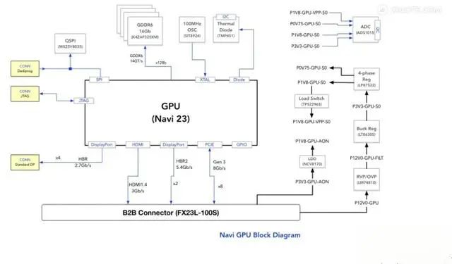
The GPU part is rumored to have a structural block diagram from Tesla, with a core being Navi 23, OPN number 215-130000026, paired with 4 pieces of Samsung dedicated GDDR6 memory, one piece of 16Gb (2GB) totaling 8GB, with a rate of 14GT/s, memory interface of 128-bit, and peripherals including power supply, JTAG debugging port, crystal oscillator, thermal sensor, etc. The GPU’s HDMI, DP, and PCIe structure are connected to the large board APU via B2B (Board to Board) connectors.
The connector model is FX23L-100S, supplied by Hirose HRS, with 100 pins and a maximum transmission rate supporting 8Gbps, capable of meeting the high-speed data transmission requirements of HDMI/DP/PCIe Gen3.
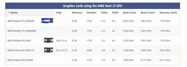
AMD Navi 23 core independent graphics card model can be referenced in the following table, with performance likely comparable to the AMD Radeon PRO W6600 graphics card, 8GB dedicated GDDR6 memory, TSMC 7nm process, 1792 stream processors, peak single precision (FP32) performance of 10.4 TFLOPs [4], and thermal design power (TDP) of 130W Peak.
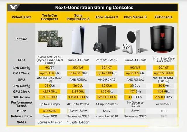
The AMD Ryzen Embedded APU, paired with the AMD RDNA 2 architecture independent graphics card, has performance comparable to current PS5 and XBOX gaming consoles [5].
The audio section selects two ADI SHARC+ high-performance floating-point ADSPs, with models SC587W and AD21584, where AD21584 is used for active road noise reduction calculations, and SC587W is paired with ARM Cortex-A5 and two RAMs.
The AMP amplifier section consists of three 4-channel output Class D amplifiers, with six groups of inductors above the amplifier for Class D output filtering, apparently supporting 12-channel output, officially announced as 960W audio power, with a total of 22 speakers, indicating a high-quality audio system. This effectively integrates an independent amplifier into the MCU, and the audio effect should be promising.
MCU, like Model 3/Y, uses SPC5748GSMMJ6 for power control and gateway communication management, etc.;
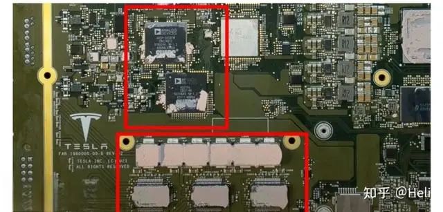
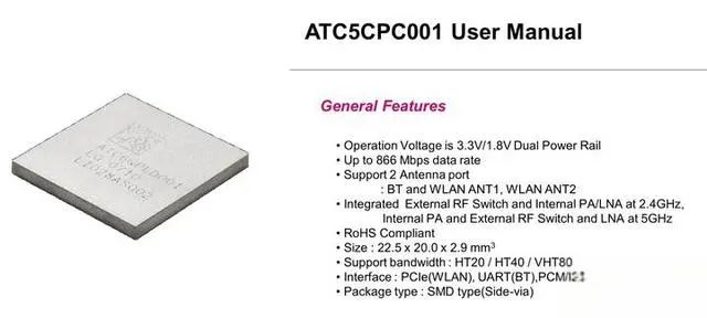
BT & WiFi are handled by LG Innotek’s BT and WiFi dual-module ATC5CPC001, supporting BT (v5.0) + 2.4GHz/5GHz WiFi 5 (802.11a/b/g/n/ac) 2×2 MIMO Module.
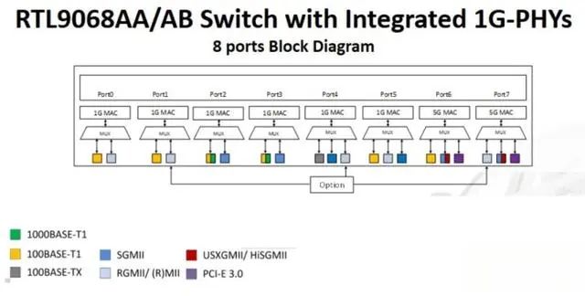
The Ethernet switch is Realtek’s RTL9068A, supporting a maximum of 8 ports, and the display serializers are likely based on TI solutions, with GPS and camera inputs placed on the AP hardware.
Model Y and Model S Plaid MCU have slight differences, with a comparative analysis saved for the next article. Below is the Ingineerix teardown video of the Model S Plaid central computing platform.
“Super Workshop” Model Y Performance vehicle machine teardown: A Brief Analysis of Tesla’s AMD Vehicle Machine.