
In embedded development, current backflow is an easily overlooked issue that can lead to serious consequences. This chapter will delve into the causes, impacts, and how to identify and prevent this issue in practical engineering.
The issue of current backflow rarely occurs during the 5V single-chip microcontroller era, mainly because the IO withstand voltage of 5V single chips is high, and the internal structure of the microcontroller is well-designed for IO protection. In the era of 3.3V microcontrollers, such problems have some occasional occurrences, but they are still rare. Although the IO withstand voltage of microcontrollers has decreased, the internal protection design is still very effective. Additionally, the time from powering on the microcontroller to program execution is very short. Once the IO ports are correctly initialized, they can match well with peripheral levels and avoid current backflow. However, with the current MPUs, the scale of processors is larger, and there are many IO ports. The system power supply usually has several different voltage paths, and there are strict power-on sequencing requirements. Coupled with the multi-stage startup of the processor, the startup time is longer. During the time from power-on to completing IO initialization, if the levels are not handled carefully, current backflow may occur.
Current backflow is a very covert issue, akin to a “chronic disease”, which is difficult to detect immediately during product use. Problems may only arise after long-term operation in the application field, and they can manifest in various ways. Even if a solution is provided, the effect is not immediate; it requires long-term operation to verify the effectiveness of the improvement plan.
If a product fails after running on-site for a long time, and the same model fails to replicate the issue in the laboratory, it can be considered to investigate whether there is current backflow in the circuit design, given that the basic positioning is a hardware issue. Based on years of application experience, the following faults/problems can be investigated for current backflow:
-
Occasional reboots or crashes after the product has been running on-site for several months; replacing the core board resolves the issue;
-
After several months of on-site operation, network anomalies occur occasionally, or IO-controlled devices behave abnormally; replacing the core board restores normal operation;
-
The system fails to boot after several months of on-site operation; replacing the core board allows it to function normally, but the faulty board still fails to start even after replacing the baseboard in the laboratory.
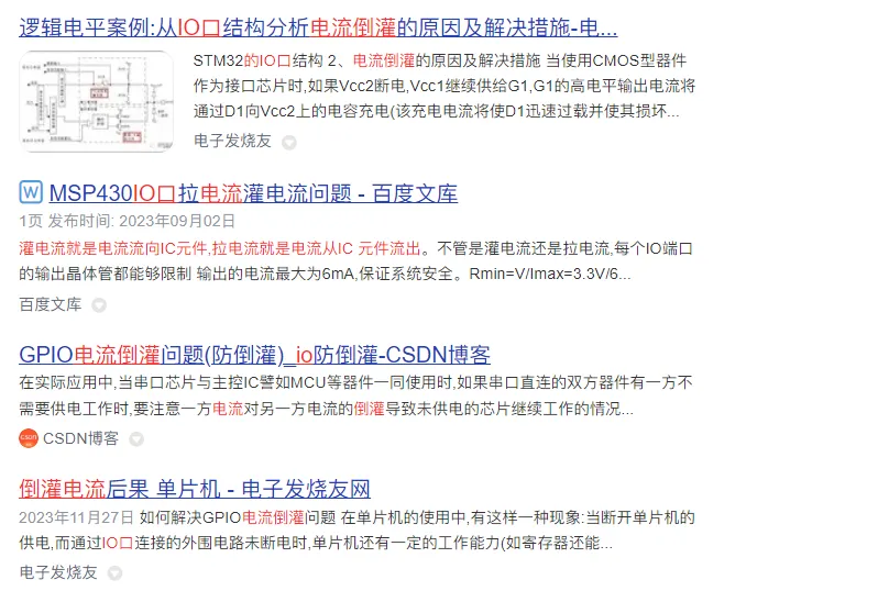
Current backflow is a common issue. Searching online with the keyword “IO current backflow” will yield many related cases and articles on solutions, as shown in Figure 1.
 Current Backflow and IO Current Backflow
Current backflow refers to the phenomenon where the direction of current flow is opposite to the conventional flow direction. In a circuit, the current typically flows from the positive terminal of the power supply, through the load, and into the negative terminal of the power supply. However, in certain cases, such as when the power supply voltage is too high, circuit protection measures are insufficient, or circuit design errors occur, the current may flow in reverse, from the negative terminal back to the positive terminal, which is referred to as current backflow.
IO current backflow refers to the phenomenon where current flows back into the chip or circuit from the power or signal lines in electronic devices. This is usually caused by improper configuration of the power or signal lines, or due to design errors in the circuit.
The consequences of current backflow can be uncertain, diverse, and covert, often making it difficult to grasp. At the mildest, it may lead to signal distortion or instability, affecting device performance and stability. At worst, one or more IOs may malfunction, or IO pins may be damaged, causing corresponding peripheral control anomalies. It can also lead to abnormal communication interfaces, and in severe cases, the system may freeze, resulting in inexplicable faults, or even damage to the CPU, necessitating repair or scrapping.
02
This article will continue to explore current backflow, analyzing the root causes of IO port damage and system stability issues in embedded systems.
 IO Port Damage
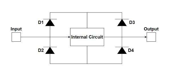
-
D1 serves as an electrostatic discharge protection in most integrated circuits while also helping to limit the input amplitude.
-
D2 is a parasitic diode generated by semiconductor integration, providing some discharge protection.
-
D3 protects the CMOS circuit from interference during discharge, and this diode is also present in most bipolar devices.
-
D4 is the parasitic diode of the collector (bipolar) or drain (field-effect transistor) of the transistor, serving a discharge function.
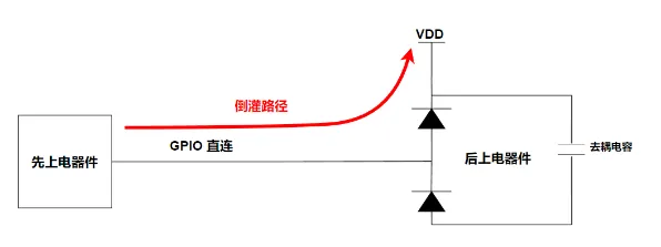
Next, we will analyze the process of current backflow damaging the IO port in conjunction with Figure 2. In a power-on sequence scenario (or when the right-side device is powered off or unplugged), if the voltage on the left side is sufficiently high, it will charge the right-side VDD through the diode, which is to charge the decoupling capacitor. This can lead to rapid overload damage to the diode and potentially damage the capacitor itself. A momentary high current can even directly destroy the component, causing even the best structures to operate incorrectly.
 System Failure
1. System Freeze or Failure to Boot
Generally, the PMU used with the SOC has an internal DC-DC that features a leakage detection function. When the PMU is not powered on, if a leakage is detected in one of the DC-DCs and the leakage voltage exceeds the VIL (TYP) value, that DC-DC will not output, causing the system to fail to boot due to the lack of voltage output from the PMU’s DC-DC. At this point, the voltage measured on the DC-DC power network is actually the leakage voltage.
If a certain DC-DC of the PMU supplies power to both the SOC and some peripherals, and many GPIOs of the SOC use the power domain of that DC-DC, the power supply for the peripherals may leak to that DC-DC through the GPIO, causing anomalies during the sleep wake-up process if the SOC chip enters sleep mode.
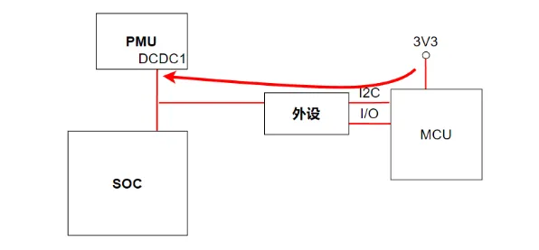
As shown in Figure 3, when the SOC chip enters sleep mode, the MCU’s I2C/UART/IO power on before DCDC1, causing the level to backflow to DCDC1 through the peripherals, resulting in sleep anomalies.
03
In the design and maintenance of electronic devices, IO current backflow is an issue that requires special attention. To prevent this phenomenon, we can take the following measures:
-
Add appropriate protective circuits or devices between the power and signal lines to ensure that current does not flow in the wrong direction.
-
Properly design and configure the circuit to reduce the risk of IO current backflow.
-
Use appropriate resistors, capacitors, diodes, and other components in electronic devices to configure the circuit and prevent current backflow.
 Case Analysis
Figure 1 shows the secondary power supply system, using the PWR_OK output from the PMU that accompanies the SOC to enable the secondary power supply, complying with the power-on sequencing requirements. The startup configuration time for the M3568 core board is approximately 200ms, and the PWR_OK signal typically rises after about 200ms of 5V power supply, ensuring that other power supplies on the baseboard are powered on only after the core board has fully powered on.
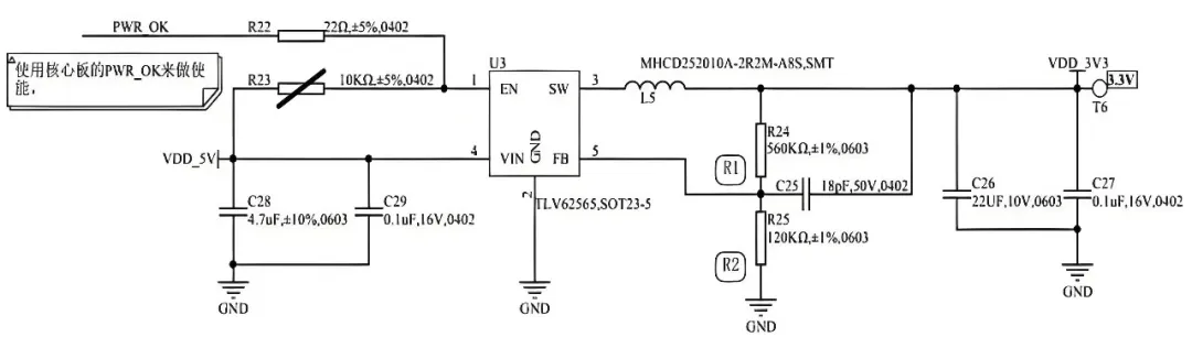
Figure 1 Secondary power supply
Case 2: The baseboard control circuit or chip pulls up the core board pin through the peripheral pull-up circuit, causing the pull-up power domain to power on before the SOC corresponding GPIO power domain, resulting in IO current backflow
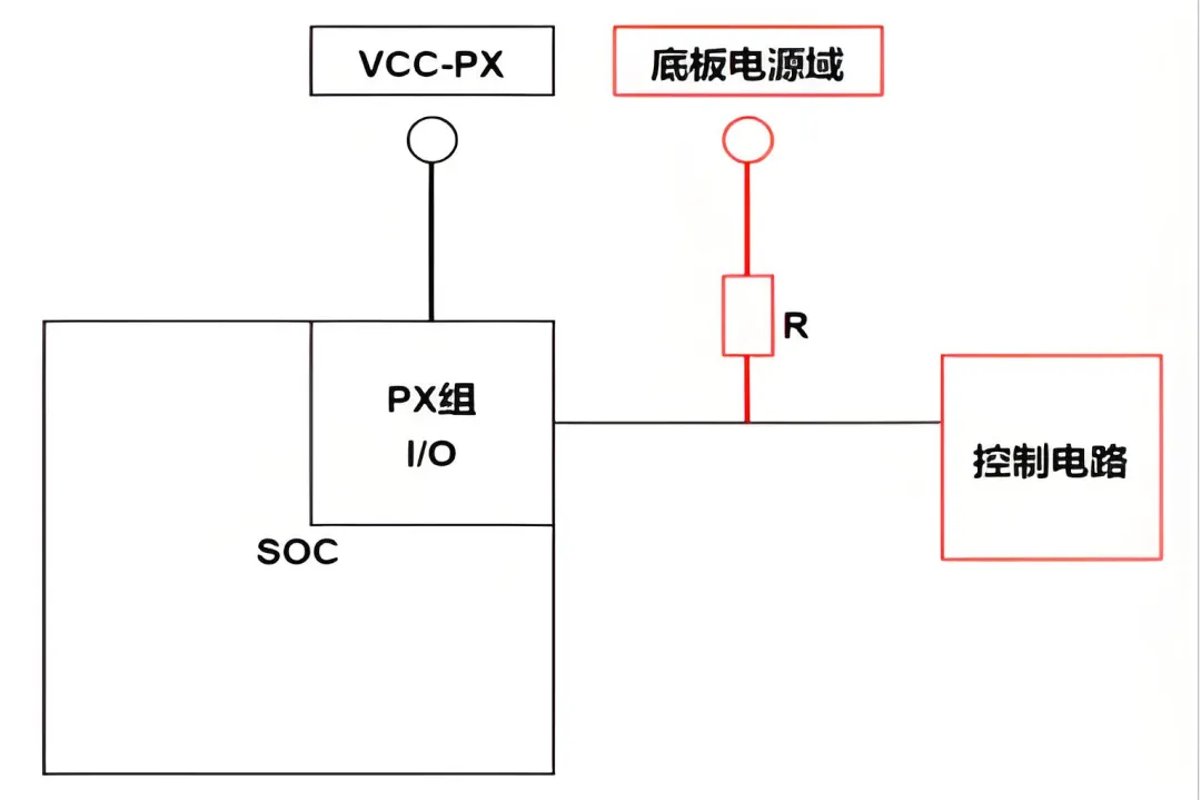
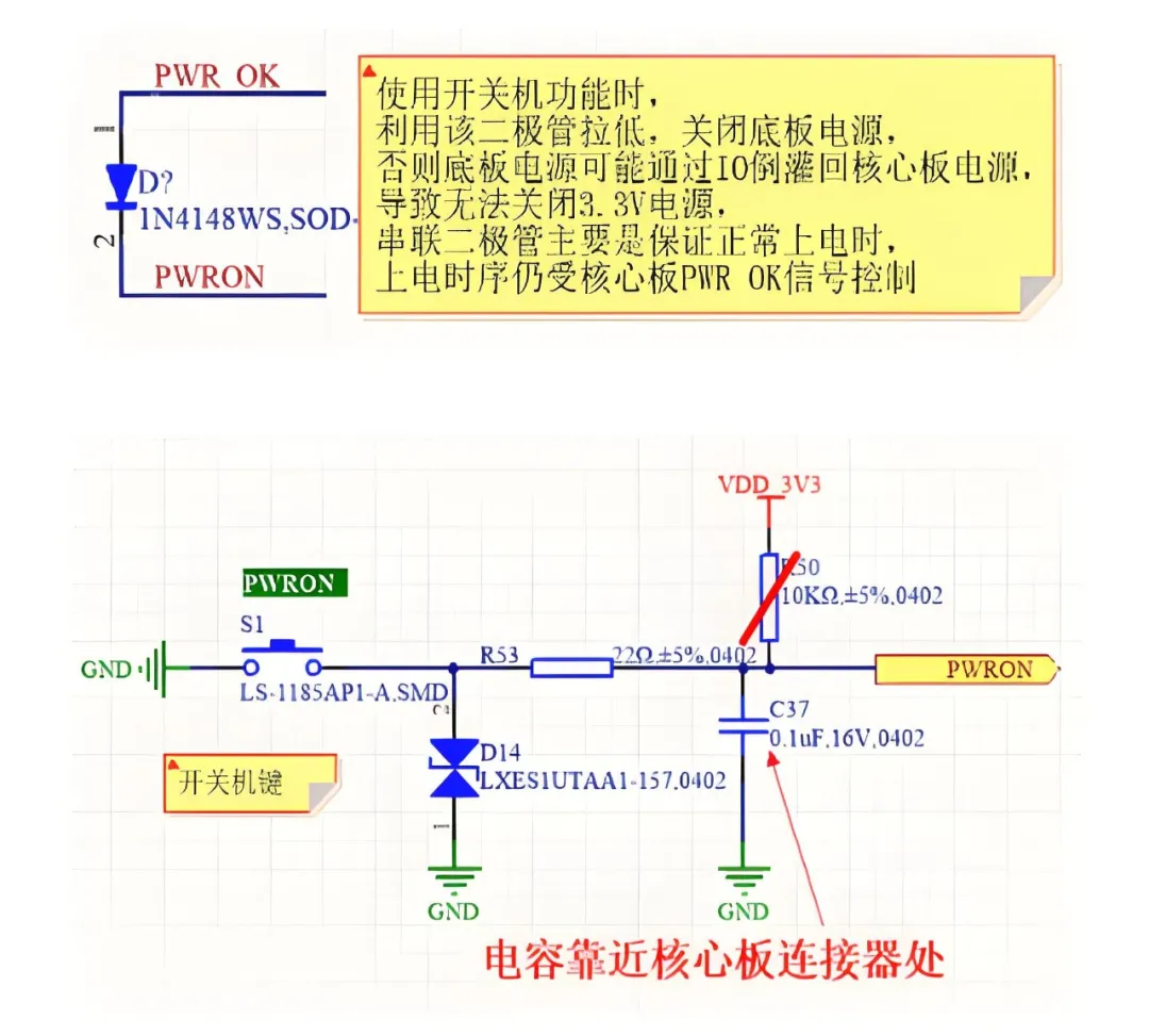
Figure 3 Power design with switch
In circuit design, one may encounter issues where the processor IO level does not match the module IO level. To ensure normal communication, level conversion is required. If directly connected, current backflow may occur, especially with TTL levels. The level conversion requirements are:
-
VOH ≥ VIH, VOL ≤ VIL;
-
For multi-power systems, certain devices do not allow input levels to exceed the power supply voltage. For chips with similar requirements, ensure appropriate protection is implemented in the circuit;
-
Level conversion can affect communication speed.
-
Left side onboard input high level, UGS=0V, NMOS off, right side output is 5V high level;
-
Left side onboard input low level, UGS=3.3V, NMOS on, right side output is onboard low level;
-
Right side interface input high level, UGS=0V, NMOS off, left side output is 3.3V high level;
-
Right side interface input low level, NMOS body diode conducts, UGS=2.6V (body diode has a forward voltage drop), as long as the NMOS gate voltage is lower than UGS, the NMOS turns on, and the left side outputs interface low level.
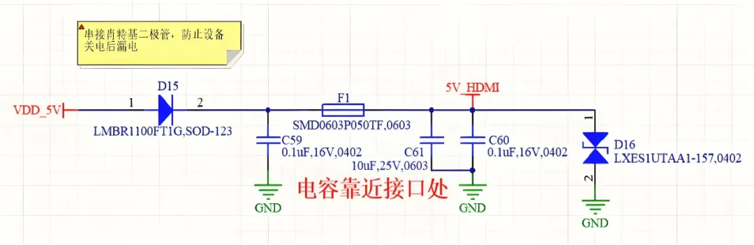
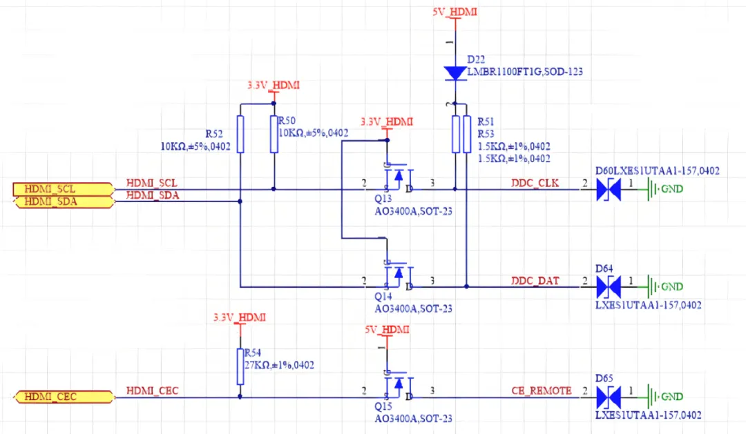
Figure 5 HDMI 5V power supply backflow prevention
Recommended Reading:
Why is a resistor often connected in series between the signal sender and receiver? What is its purpose?
What happens if a CAN bus does not have a terminal resistor?
To play with hardware, you need a good set of equipment! See what you lack compared to the experts?
Why are NMOS transistors more popular than PMOS transistors?
A common circuit for reverse connection protection, soft start, and overvoltage protection