 Research Special Issue on Emerging Computing Chip Design
With the rapid development of information technology, artificial intelligence, big data, cloud computing, and the Internet of Things, the global demand for computing performance, energy efficiency, and intelligence continues to rise. Traditional chip architectures struggle to meet the requirements for high performance, low power consumption, and high concurrency when faced with complex, massive, and diverse data processing tasks. At the same time, as Moore’s Law slows down and the benefits of process miniaturization gradually diminish, the path of relying on traditional process technologies to drive performance improvements faces significant challenges. There is an urgent need to explore new architectures and design methods to break through performance bottlenecks and achieve continuous evolution and innovative development. Emerging computing chip design, as a key technological route to break the limitations of traditional architectures and enhance overall computing power and system energy efficiency, is becoming a frontier direction of interest in both the international academic and industrial communities.
To comprehensively showcase the latest academic achievements and technological advancements in the field of emerging computing chip design, the 2025 Issue 8 of “Integrated Circuits and Embedded Systems” has specially planned a “Research Special Issue on Emerging Computing Chip Design.” The content covers key technologies in high-efficiency emerging memory in-memory computing, hyperdimensional computing hardware design technologies, dedicated SoC architectures for large models and multi-agent tasks, chip optimization schemes in low-temperature environments, on-chip network communication interfaces, and cache coherence mechanisms, as well as efficient convolution acceleration technologies. These studies not only focus on innovations in new devices and architectures but also consider system-level optimization needs such as high energy efficiency, low power consumption, and flexible adaptability, fully demonstrating the multidimensional exploration and continuous breakthroughs of Chinese research teams in the field of emerging computing chips, highlighting their strong technological innovation capabilities and application prospects.
The following 9 articles are included (click to read the full text or download the complete PDF version):
Hyperdimensional Computing Hardware Design: Progress, Trends, and Prospects
A Review of ROM-SRAM Hybrid In-Memory Computing Architecture
A Review of Low-Temperature In-Memory Computing Chip Design
End-to-End Domain-Specific SoC Design Based on Large Language Model Multi-Agent
Efficient Winograd Convolution Hardware Design and Its Quantization Scheme
Research on Time Domain In-Memory Computing Method for Spin Transfer Torque Magnetic Random Access Memory
A Communication Interface Design for NoC and Flash Controller
Design and Implementation of PCIe RP System Based on Cortex-M3 Kernel
Using Multicast Adaptive Routing to Accelerate the Snooping and Snooping Response Process of Cache Coherent Network on Chip
 01Hyperdimensional Computing Hardware Design: Progress, Trends, and Prospects
Tianyang Yu1,2, Bi Wu1,2, Ke Chen1,2, Weiqiang Liu1,2
(1. Nanjing University of Aeronautics and Astronautics, School of Integrated Circuits; 2. Key Laboratory of Aerospace Integrated Circuits and Microsystems, Ministry of Industry and Information Technology)
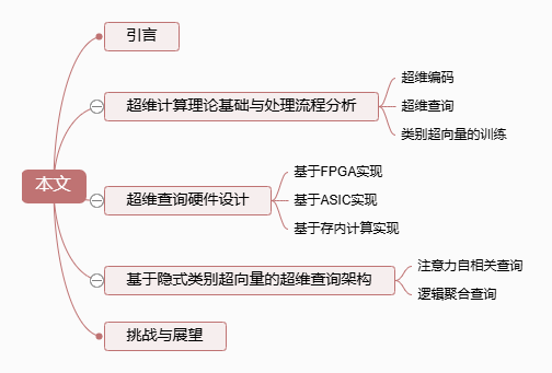
Abstract: Hyperdimensional computing is an emerging computing paradigm inspired by the human brain, characterized by low complexity, strong robustness, and strong interpretability, with broad application prospects in edge applications. Hyperdimensional computing simulates the information processing mechanism of the human brain, utilizing hyperdimensional vectors and simple logical operations to achieve complex cognitive functions, replacing the multi-layer complex structure of neural networks with a lightweight coding query process, providing a new technical path for high-energy-efficiency edge artificial intelligence chips. This paper systematically elaborates on the theoretical foundations and algorithm evolution of hyperdimensional computing and discusses the feasibility of hardware acceleration for each step. Based on this, it provides a detailed introduction to dedicated hardware focusing on the query step, summarizing three implementation methods: FPGA, ASIC, and in-memory computing, and analyzing the advantages and disadvantages of each method. Furthermore, it introduces some recent research progress addressing the common shortcomings of existing hyperdimensional query hardware. Finally, it presents the challenges faced by current hyperdimensional computing hardware and prospects for future research directions.
Citation format: Yu T Y, Wu B, Chen K, et al. Hyperdimensional computing hardware: progress, trends and prospects[J]. Integrated Circuits and Embedded Systems, 2025, 25(8): 1-9. YU T Y, WU B, CHEN K, et al. Hyperdimensional computing hardware: progress, trends and prospects[J]. Integrated Circuits and Embedded Systems, 2025, 25(8): 1-9 (in Chinese).
 02A Review of ROM-SRAM Hybrid In-Memory Computing Architecture
Xirui Du, Guodong Yin, Yiming Chen, Ling’an Zeng, Tianyi Yu, Huazhong Yang, Xueqing Li
(Tsinghua University, Department of Electronic Engineering, Flexible Electronics Technology Laboratory / National Research Center for Information Science and Technology / National Key Laboratory of Space-Based Networks and Communications)
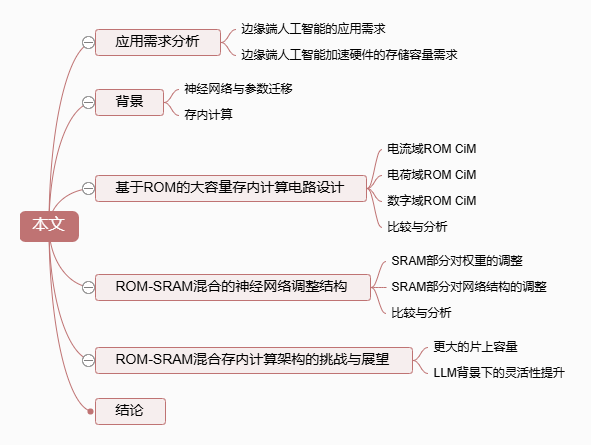
Abstract: Neural networks are representative algorithms of artificial intelligence; however, their large parameter count poses new challenges for hardware deployment at the edge. On the edge, there is a need for computing hardware to achieve task migration through fine-tuning of model parameters for application flexibility, while also requiring large on-chip storage to reduce off-chip memory access overhead for energy efficiency and performance. The recently proposed ROM-SRAM hybrid in-memory computing architecture is a promising solution under mature CMOS processes. Thanks to high-density ROM in-memory computing, most of the weights of neural networks can be deployed on-chip without relying on off-chip memory; at the same time, SRAM in-memory computing can provide flexibility for edge in-memory computing based on high-density ROM. To expand the design and application space of the ROM-SRAM hybrid in-memory computing architecture, it is necessary to further increase the density of ROM in-memory computing to support larger networks and explore solutions that achieve greater flexibility through a small amount of SRAM in-memory computing. This paper introduces several common methods to enhance the density of ROM in-memory computing and discusses methods for neural network fine-tuning based on the ROM-SRAM hybrid in-memory computing architecture to improve flexibility, as well as deployment solutions for ultra-large-scale neural networks and solutions to the dynamic matrix multiplication bottleneck encountered in long-sequence large language models, looking forward to the broad design space and application prospects of the ROM-SRAM hybrid in-memory computing architecture.
Citation format: Du X R, Yin G D, Chen Y M, et al. A review on ROM-SRAM hybrid compute in memory architecture[J]. Integrated Circuits and Embedded Systems, 2025, 25(8): 10-22. DU X R, YIN G D, CHEN Y M, et al. A review on ROM-SRAM hybrid compute in memory architecture[J]. Integrated Circuits and Embedded Systems, 2025, 25(8): 10-22 (in Chinese).
 03A Review of Low-Temperature In-Memory Computing Chip Design
Yuhao Shu1, Yifei Li2, Jincheng Wang2, Weiqiang Liu1, Yajun Ha2
(1. Nanjing University of Aeronautics and Astronautics, School of Integrated Circuits; 2. Shanghai University of Science and Technology, School of Information Science and Technology)
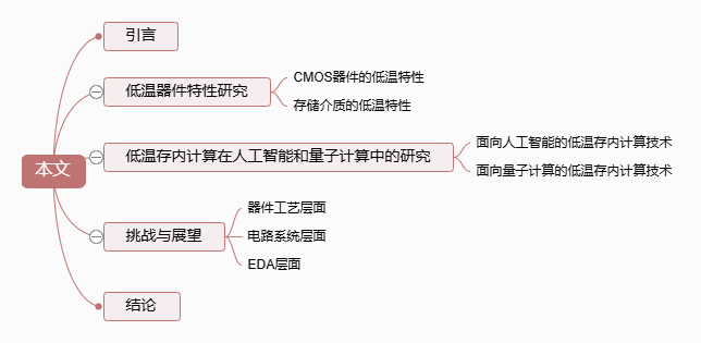
Abstract: With the rapid development of cutting-edge technologies such as artificial intelligence and quantum computing, the demand for high-performance computing chips continues to rise. However, the traditional von Neumann architecture is increasingly unable to meet the computing power requirements of data-intensive applications due to factors such as the memory wall and power wall. Low-temperature in-memory computing combines the excellent electrical characteristics of low-temperature CMOS devices with the high bandwidth and low latency advantages of in-memory computing architectures, providing a new solution to break through computing power bottlenecks. This paper reviews the key characteristics of CMOS devices and various storage media in low-temperature environments, systematically organizes the typical architectures, key implementations, and performance of low-temperature in-memory computing in the fields of artificial intelligence and quantum computing, and analyzes the challenges and future development trends at the levels of device processes, circuit systems, and EDA tools.
Citation format: Shu Y H, Li Y F, Wang J C, et al. Review on cryogenic in memory computing chip design[J]. Integrated Circuits and Embedded Systems, 2025, 25(8): 23-30. SHU Y H, LI Y F, WANG J C, et al. Review on cryogenic in memory computing chip design[J]. Integrated Circuits and Embedded Systems, 2025, 25(8): 23-30 (in Chinese).
 04End-to-End Domain-Specific SoC Design Based on Large Language Model Multi-Agent
Peiran Yan, Qinzhe Zhi, Lifeng Liu, Tianyu Jia
(Peking University, School of Integrated Circuits)
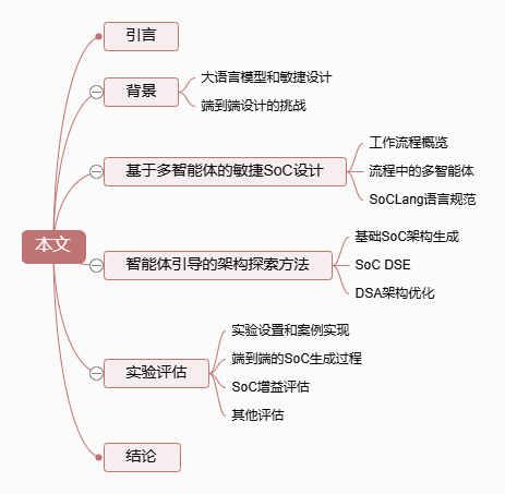
Abstract: With the slowdown of Moore’s Law, domain-specific system-on-chip (DSSoC) integration of domain-specific accelerators (DSA) has become a highly promising energy-efficient chip design strategy. However, the design process of DSSoC is highly complex, leading to long development cycles and significant human resource investment. Recent advancements in large language models (LLMs) have introduced new methods for agile chip design, demonstrating great application potential in code generation and EDA script writing. This paper proposes an LLM-based multi-agent DSSoC design framework that covers the end-to-end design process from architecture definition to code generation and EDA physical implementation. Finally, two case studies validate that this framework can complete two SoC designs in just 2 to 4 weeks at 22 nm and 7 nm process nodes. Compared to SoCs generated by the original process, the SoCs designed using this method achieved energy efficiency improvements of 4.84 times and 3.82 times, respectively.
Citation format: Yan P R, Zhi Q Z, Liu L F, et al. End to end domain specific SoC design with LLM based multi agent[J]. Integrated Circuits and Embedded Systems, 2025, 25(8): 31-40. YAN P R, ZHI Q Z, LIU L F, et al. End to end domain specific SoC design with LLM based multi agent[J]. Integrated Circuits and Embedded Systems, 2025, 25(8): 31-40 (in Chinese).
 05Efficient Winograd Convolution Hardware Design and Its Quantization Scheme
Zheng Yan, Chenshuo Zhang, Yichuan Bai, Yuan Du, Li Du
(Nanjing University, School of Electronic Science and Engineering)
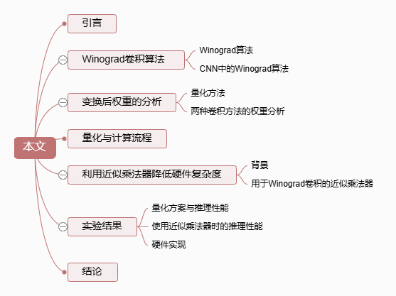
Abstract: Convolution is a common operation in CNN networks, and the multiply-accumulate operations in convolution consume significant power, limiting the performance of many CNN hardware accelerators. Reducing the number of multiplications in convolution is one effective way to improve CNN accelerator performance. As a fast convolution algorithm, the Winograd algorithm can reduce up to 75% of multiplications in convolution. However, the weight distribution in Winograd convolution is significantly different, leading to the need for longer quantization bit widths to maintain similar accuracy, which offsets the hardware optimization benefits gained from reducing the number of multiplications. This paper conducts a quantitative analysis of this issue and proposes a new quantization scheme for Winograd convolution, achieving less than 1% accuracy loss. To further reduce hardware costs, approximate multipliers are applied to Winograd convolution. Compared to traditional convolution computing blocks, the Winograd computing block saves 27.3% area, and the application of approximate multipliers in the Winograd computing block saves 39.6% area, with negligible performance loss.
Citation format: Yan Z, Zhang C S, Bai Y C, et al. Design of efficient Winograd convolution hardware and its quantization scheme[J]. Integrated Circuits and Embedded Systems, 2025, 25(8): 41-52. YAN Z, ZHANG C S, BAI Y C, et al. Design of efficient Winograd convolution hardware and its quantization scheme[J]. Integrated Circuits and Embedded Systems, 2025, 25(8): 41-52 (in Chinese).
 06Research on Time Domain In-Memory Computing Method for Spin Transfer Torque Magnetic Random Access Memory
Jiahui Tan1, Jiongzhe Su2, Rong Zhou2, Chunzhang Zhang3, Hao Cai2
(1. Southeast University, Wu Jianxiong College; 2. Southeast University, School of Integrated Circuits; 3. Southeast University, School of Electronic Science and Engineering)
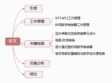
Abstract: In-memory computing based on spin-transfer torque magnetic random access memory (STT MRAM) is expected to be an effective way to overcome the “memory wall” bottleneck. This paper proposes a high-energy-efficient in-memory computing design scheme suitable for STT MRAM based on the time domain: a custom series storage unit structure that forms a magnetic resistance chain of multiple rows of storage units in series during the computing mode by connecting transistors and complementary MTJs, combined with a time domain conversion circuit that converts resistance values into pulse delay signals. Furthermore, a complementary series array architecture is designed, which generates differential time signals by storing positive and negative weights separately, supporting signed number calculations. In terms of quantization circuit design, a successive approximation register (SAR) time-to-digital converter (TDC) is proposed, which adopts a structure combining voltage-adjustable delay chains and flip-flops. To achieve multi-bit multiply-accumulate operations, a signed weight encoding scheme and digital post-processing architecture are proposed, which decompose the multiplication and accumulation of 8-bit inputs and 8-bit weights into low 5-bit time domain calculations and high-bit digital domain calculations, outputting a 21-bit full-precision result. Based on 28 nm CMOS technology, layout design and post-simulation are completed, achieving a resolution margin of 270 ps for 9-bit multiply-accumulate operations at a voltage of 0.9 V, with an energy consumption of only 16 fJ per operation. The designed 9 Kb time domain storage macro unit, with an area of 0.026 mm2, includes a storage unit array, SAR TDC module, computing circuit, and read/write control circuit. The macro unit can achieve energy efficiencies of 26.4 TOPS/W and 42.8 TOPS/W when performing convolution layer calculations and fully connected layer calculations, respectively, while achieving an area efficiency of 0.523 TOPS/mm2 at 8-bit precision calculations.
Citation format: Tan J H, Su J Z, Zhou R, et al. Research on time domain in memory computing method for spin transfer torque magnetic random access memory[J]. Integrated Circuits and Embedded Systems, 2025, 25(8): 53-63. TAN J H, SU J Z, ZHOU R, et al. Research on time domain in memory computing method for spin transfer torque magnetic random access memory[J]. Integrated Circuits and Embedded Systems, 2025, 25(8): 53-63 (in Chinese).
 07A Communication Interface Design for NoC and Flash Controller
Qingxin Li1,2,3, Jinghe Wei1,2,3, Ying Gao1,2,3, Yujie Han1,2,3, Hu Ju1,2,3, Shujun Cai1,2, Jianfei Jiang4
(1. National Key Laboratory of Integrated Circuits and Microsystems; 2. China Electronics Technology Group Corporation No. 58 Research Institute; 3. Key Laboratory of Aerospace Integrated Circuits and Microsystems, Ministry of Industry and Information Technology; 4. Shanghai Jiao Tong University)
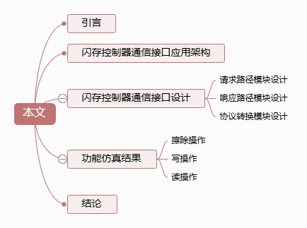
Abstract: A communication interface designed for NoC and flash controllers mainly includes request path modules, protocol conversion modules, and response path modules. The request path module can complete data verification and cross-clock domain processing for request data packets sent by the NoC, while the protocol conversion module converts the processed data packets into configuration instructions in the form of AHB bus signals to configure the flash controller, thereby controlling the flash storage device to perform erase, read, and write operations. When the flash storage device generates response data, the protocol conversion module packages the received response data into response data packets, which are fed back to the NoC via the response path module. This communication interface can improve the data packet transmission efficiency between the NoC and flash controller, solving the problem of efficient transmission interaction of data packets among multi-chiplets, providing a technical foundation for the development of multi-chiplet integration technology.
Citation format: Li Q X, Wei J H, Gao Y, et al. A communication interface design for NoC and Flash controller[J]. Integrated Circuits and Embedded Systems, 2025, 25(8): 64-73. LI Q X, WEI J H, GAO Y, et al. A communication interface design for NoC and Flash controller[J]. Integrated Circuits and Embedded Systems, 2025, 25(8): 64-73 (in Chinese).
 08Design and Implementation of PCIe RP System Based on Cortex-M3 Kernel
Junjie Xu, Jinghe Wei, Guozhu Liu, Jian He, Zheng Zhang
(National Key Laboratory of Integrated Circuits and Microsystems)
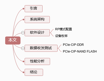
Abstract: Peripheral Component Interconnect Express (PCIe) and Serial Rapid IO (SRIO) are mainstream high-speed communication interface protocols. In application scenarios characterized by large data volumes, such as those represented by artificial intelligence, achieving compatibility with these protocols is key to building high-performance systems and breaking through storage and computing bottlenecks. To meet this demand, the Chiplets Interconnect Protocol (CIP) implements multi-protocol conversion interactions among PCIe, SRIO, DDR, and NAND FLASH through a unified routing network. Among them, PCIe serves as the primary human-computer interaction interface, and building a PCIe RP (Root Port) system is fundamental to achieving PCIe communication. Existing PCIe read/write devices based on operating systems suffer from high latency and poor operability. To address these issues, a PCIe RP system based on the Cortex M3 processor has been established, along with corresponding driver and software development, achieving efficient and accurate data transmission between PCIe and various devices. Based on the basic functionality, stability tests for large-scale data interactions of 50,000, 100,000, and 150,000 times were completed. The results indicate that this system exhibits good stability in large-scale data interaction events, providing a solution for data interaction between processors and PCIe.
Citation format: Xu J J, Wei J H, Liu G Z, et al. Design and implementation of PCIe RP system based on Cortex-M3 kernel[J]. Integrated Circuits and Embedded Systems, 2025, 25(8): 74-80. XU J J, WEI J H, LIU G Z, et al. Design and implementation of PCIe RP system based on Cortex-M3 kernel[J]. Integrated Circuits and Embedded Systems, 2025, 25(8): 74-80 (in Chinese).
09Using Multicast Adaptive Routing to Accelerate the Snooping and Snooping Response Process of Cache Coherent Network on Chip
Dongwei Hu1, Xiaohui Ba2, Gengting Liu3, Linan Wang1, Yuejun Lei4
(1. China Electronics Technology Group Corporation No. 54 Research Institute; 2. Beijing Jiaotong University, School of Electronic Information Engineering; 3. University of Manchester, Department of Computer Science; 4. Minzu University of China, School of Information Engineering)
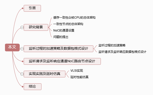
Abstract: To address the excessive time consumption of the snooping and snooping response process in cache coherent networks on chip (NoC) in many-core CPU chips, this paper proposes two techniques: multicast and adaptive routing to accelerate this process. Based on the requirements of these two techniques, the packet formats for NoC snooping requests and snooping response data are designed, and further designs and implementations of NoC routers for snooping request channels and snooping response channels, as well as an 8×8 network, are carried out. Design practices show that the proposed NoC router has sizes of 85,940.3 μm2 or 103,518.5 μm2 under 22 nm technology, and the sizes of the 8×8 snooping request and snooping response networks are 5.57 mm2, with acceptable complexity. Simulation experiments compared the time consumption of the snooping and snooping response processes under four configurations: unicast and multicast, deterministic routing and adaptive routing. The results indicate that when a snooping request message needs to snoop all 252 processor cores, the proposed techniques can reduce the time consumption of one snooping request message’s snooping and snooping response process by 45%, which is significantly lower than the access latency of DDR/HBM. If the Outstanding technique is further employed at the Point of Coherency (PoC), the proposed techniques can reduce the time consumption of 32 snooping request messages’ snooping and snooping response processes by 73%. Simulation results confirm the effectiveness of the proposed multicast and adaptive routing techniques.
Citation format: Hu D W, Ba X H, Liu G T, et al. Accelerating the snooping & snooping response process of cache coherent network on chip with multicast adaptive routing[J]. Integrated Circuits and Embedded Systems, 2025, 25(8): 81-90. HU D W, BA X H, LIU G T, et al. Accelerating the snooping & snooping response process of cache coherent network on chip with multicast adaptive routing[J]. Integrated Circuits and Embedded Systems, 2025, 25(8): 81-90 (in Chinese).

Special Issue Editor
Weiqiang Liu
Executive Dean and Professor of the School of Integrated Circuits, Nanjing University of Aeronautics and Astronautics, National Distinguished Young Scholar. Currently serves as a member of the overall expert group of the National Key R&D Program “Micro-Nano Electronic Technology”, director of the “Aerospace Integrated Circuits and Microsystems” key laboratory of the Ministry of Industry and Information Technology, vice-chair of the IEEE Nanotechnology Council (NTC), chair of the IEEE TVLSI journal advisory committee, and Fellow of the Institution of Engineering and Technology (IET). He has led major research projects supported by the National Natural Science Foundation, the Basic Strengthening Program, and other projects. He has published three English monographs and over 100 papers in Proceedings of the IEEE and IEEE journals. He has led the team to win the first prize of Jiangsu Provincial Science and Technology Award, the 18th Huoyingdong Young Scientist Award, the Huawei Technology Achievement Transformation Award, and the Excellent Cooperation Award, and has been selected as one of the top 2% scientists globally (Lifetime Impact List).

Special Issue Editor
Ke Chen
Associate Researcher at Nanjing University of Aeronautics and Astronautics, Jiangsu Province “Double Innovation Doctor”. Engaged in research on emerging computing circuit design, serving as a member of the IEEE Circuits and Systems Society VLSI Systems Applications Technical Committee and executive member of the CCF Fault-Tolerant Computing Committee. He has undertaken projects from the National Natural Science Foundation, the Key R&D Young Scientist Program, and the Basic Strengthening Program. He has published over 50 papers in authoritative journals and academic conferences in the fields of IEEE TC, TCAS-I, TETC, TVLSI, DAC, DATE, and Chinese Science – Information Science. He serves as the editor of the IEEE Nanotechnology Committee Newsletter, guest editor for journals such as IEEE TETC and IEEE TCAS-I, and a member of the TPC for international conferences such as ASP-DAC, ISCAS, GLSVLSI, and ASAP. He has received the Huawei Technology Achievement Transformation Award and the Excellent Cooperation Award.
PreviousIssuesContents: