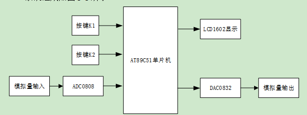
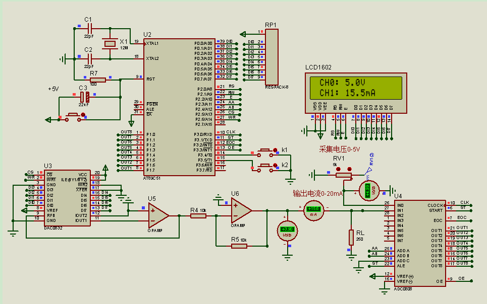
A/DConversion Circuit
1 Selection
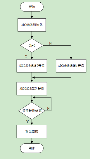
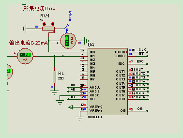
Voltage and current acquisition and AD conversion circuit uses ADC0808 as the AD conversion chip. It is a successive approximation type A/D converter that can be directly connected to the microcontroller pins.ADC0808 can collect 8 channels of voltage, and through AT89C51 control of the ADC0808 pins, it can achieve ADC0808 channel switching and AD conversion functionality.
2 ADC0808 Function Introduction
VCC : Connect to the positive terminal of the 5V power supply.
GND : Connect to ground.
OUT1–OUT8 : 8-bit digital output pins after AD conversion.
IN0-IN7 : 8 bit analog input pins, with an input voltage range of 0~5V, connected to the microcontroller’s P0 port.
ALE, START : Address latch enable signal and conversion start signal input terminals.
CLK : Chip clock input, clock frequency is generally 500KHz.
EOC : ADC0808 conversion end signal port, during AD conversion, this pin is low level, after conversion ends, the EOC pin outputs high level.
OE : Output enable signal, data can only be output when OE is low level. In the program, first set OE to 0, then to 1, thus sending the data to the microcontroller’s P0 port.
VREF+/VREF- : respectively connect to the positive and negative terminals of the reference voltage.
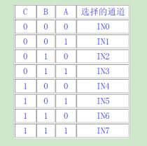
ADD A, ADD B, ADD C : Analog input channel selection terminals, used to control IN0-IN7 channel conduction. The channel selection table is as follows:
ADC0808 voltage and current acquisition circuit is as follows:
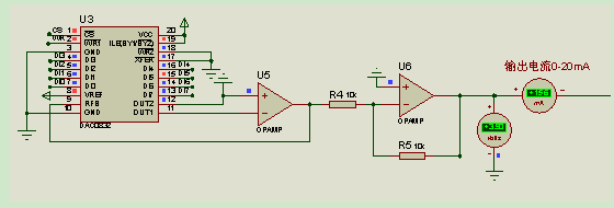
D/AConversion Circuit
1 Selection
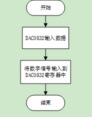
D/A conversion circuit selects the DAC0832 chip, DAC0808 chip is an 8 bit digital-to-analog conversion integrated chip, data input can use double buffering, single buffering, or direct connection methods, current output, output current linearity can be adjusted under full scale.
2 DAC0832 Function Introduction
DI0-DI7 : 8 bit parallel data input terminals.
RFB : Feedback signal input line, the chip has internal feedback resistance.
IOUT1: Current output terminal, when the input is all 1, the current is maximum.
IOUT2 : Current output terminal, its value is constant withIOUT1 terminal current.
ILE, CS, WR1 : Among them, ILE is the data latch enable input terminal, high level effective. CS is the chip select signal, low level effective. WR1 is the write selection signal for the input register, low level effective. When ILE=1, CS=0, WR1=0, the internal first stage of DAC0832’s 8 bit input register is selected. The digital signal to be converted is latched into the first stage 8 bit input register.
XFER, WR2 : Among them, XREF is the data transfer control signal input terminal, low level effective. WR2 is the write selection input terminal for the DAC register, low level effective. When XFER=0, WR2=0, the digital signal waiting to be converted in the internal first stage of DAC0832’s 8 bit input register enters the second stage’s 8 bit DAC register.
WR2 : DAC register’s write selection input terminal, negative pulse effective (pulse width greater than 500ns), when XREF is 0 and WR2 is effective, the data register’s state is transmitted to the DAC register.
VREF : Reference voltage input line, the voltage range that can be connected is-10v~+10v.
DAC0832 output voltage and current circuit is as follows:
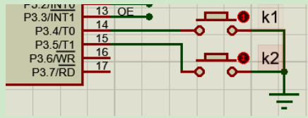
Key Circuit
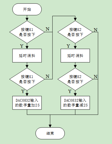
The key circuit consists of 2 independent keys, adding a keyboard module for convenient human-computer interaction, making it easy to adjust working conditions. Among them, K1 is used to increase the output current value of DAC0832, K2 is used to decrease the output current value of DAC0832. The key circuit connection is as follows:
Overall Circuit Diagram
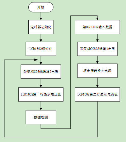
Main Program Flowchart