Click to listen while watching☝ (Today’s recommendation: “Unforgettable Samba”)
In radio frequency communication systems, signal attenuation occurs due to factors like obstacles and air effects, necessitating the ability to process data conversion over the maximum range. Based on this consideration, automatic gain control (AGC) circuits are typically used at the front end of standard RF systems. They perform functions such as receiving signal strength indicator (RSSI) detection and automatic control of intermediate frequency signal gain.
The AGC circuit adjusts the link gain by detecting the signal strength. Based on the detected signal, it is generally divided into feedback and feedforward structures. The feedforward AGC circuit detects the input signal amplitude and adjusts the gain; the feedback AGC circuit detects the output signal amplitude and adjusts the gain. Due to its higher linearity, feedback AGC circuits are more widely used. However, feedforward AGC circuits can operate over a broader bandwidth and have shorter stabilization times.
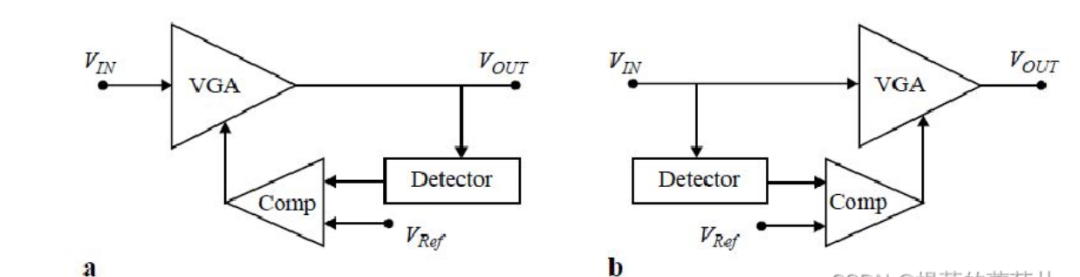
Figure a shows the feedback AGC, and figure b shows the feedforward AGC.
Advantages of feedback AGC:
1. Due to stability limitations, the dynamic range of feedback AGC circuits will not be very high, so the requirements for peak detectors are not stringent, as long as they meet the gain control needs, which are the same as the gain range of the VGA.
2. The linearity is higher due to the feedback structure, but when the input signal changes significantly, deep negative feedback can become a stability issue.
3. To ensure stability, the feedback loop has maximum bandwidth requirements for the signal, which imposes minimum requirements on loop stabilization time. When using a feedback structure, to maintain a constant stabilization time, specific requirements for the control voltage function are generally needed, meaning that the VGA gain must satisfy an exponential linear relationship with the control signal.
Feedforward AGC does not form a feedback loop and has no stability requirements, allowing it to handle large signal variations (increases or decreases) without changing stabilization time. The stabilization time of feedforward AGC only depends on the signal detection branch (which has filtering stages, leading to a larger RC delay), so there is no trade-off between stability and dynamic range. However, the detection range of the feedforward AGC structure generally needs to encompass the entire input signal dynamic range, and without feedback assurance, the requirements for linearity are higher.
The commonly used mode is the feedback AGC circuit.
1. Significance of AGC Circuit
The purpose of the AGC circuit is to allow the receiver’s gain to automatically adjust according to the strength of the input signal, keeping the amplitude of useful signals constant or varying within a specific range after AGC processing. AGC ensures that when receiving weak signals, the receiver gain increases, while when receiving strong signals, the gain decreases, thereby keeping the output signal at an appropriate level, preventing the receiver from failing to operate due to excessively weak input signals or from saturating or blocking due to excessively strong input signals.
Without an automatic gain control circuit, it is likely that the receiver will saturate or overload when receiving very strong or very weak signals, or that the signal will be drowned in noise, leading to receiver malfunction. Under the control of the automatic gain control circuit, the performance of the entire system can be guaranteed, allowing the next stage of the circuit to operate normally. Automatic gain control circuits are widely used in optical fiber communication, microwave communication, satellite communication systems, as well as in radar and broadcasting systems. Thus, the automatic gain control circuit holds a very important position in receivers.
2. Implementation Forms of AGC Circuit
Common AGC circuit functions have two implementation forms:
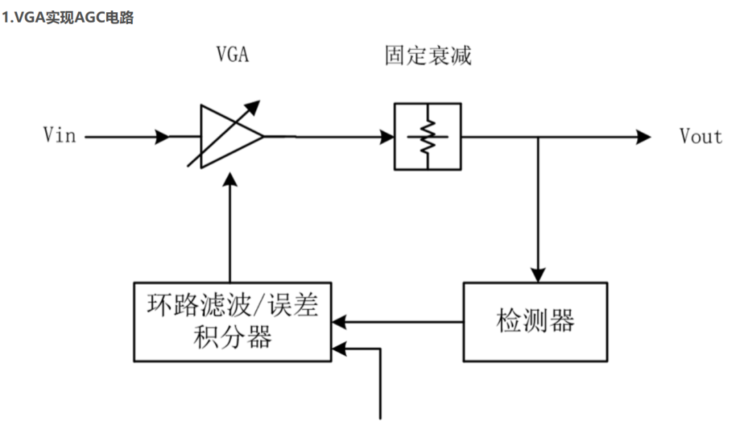
1. Variable Gain Amplifier (VGA) for dynamic range, adding a fixed attenuator to adjust the starting level of the dynamic range.
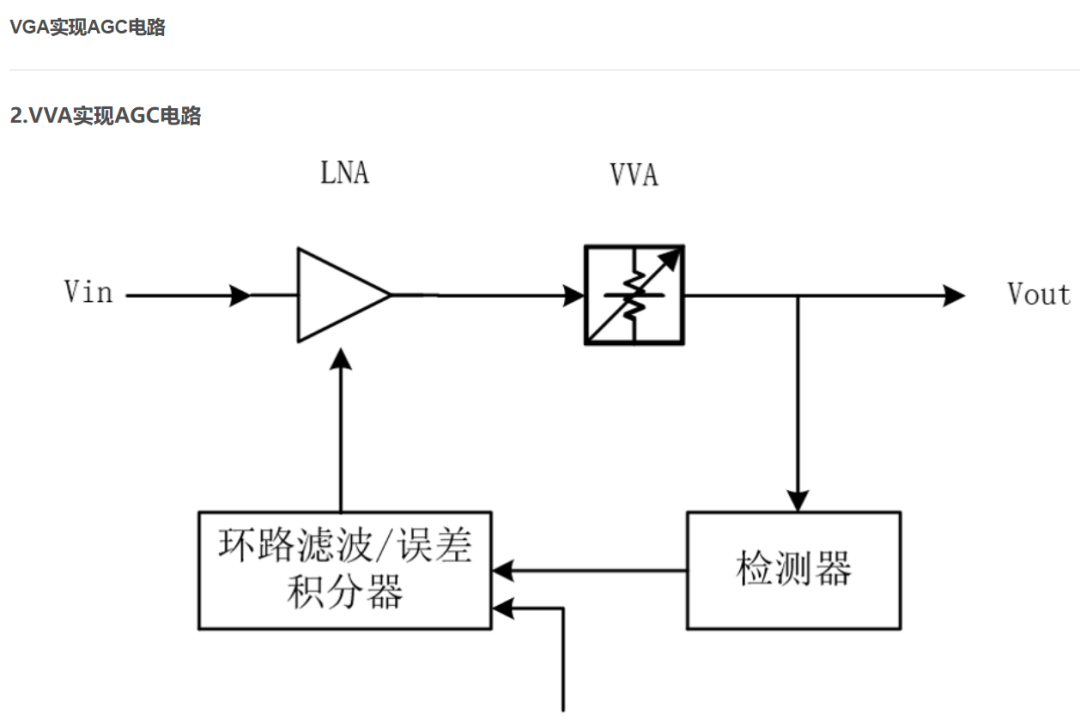
2. Voltage Variable Attenuator (VVA) for dynamic range, adding a fixed gain amplifier to adjust the starting level of the dynamic range.
The former usually has a smaller bandwidth and lower frequency, but if there is a suitable VGA, the circuit implementation is simple. The latter can be applied over a wider range, with numerous VVA and low-noise amplification products across various frequency bands. However, the overall implementation requires many components, making the circuit more complex.
3. Circuit Composition
(1) AGC Loop Stabilization Time
The AGC loop stabilization time is one of the key indicators of the AGC system; it characterizes the time taken for the AGC loop output to transition from a non-steady state to a steady state when the strength of the input signal changes. Generally, under the condition of smooth slow fading, the loop stabilization time should be much greater than the modulation rate of the information, but less than the power variation rate defined by the communication system. It should not be too short or too long to avoid frequency distortion caused by the loop stabilization time being too short, leading to bit errors; or because the loop stabilization time is too long to keep up with the changes in the input signal level, resulting in the output signal amplitude exceeding the ADC amplitude range and causing bit errors.
To achieve error-free recovery of data from the input signal, the AGC circuit needs to adjust the amplitude of the input signal to a specific range. The amplitude acquisition process generally occurs during the pre-synchronization signal, with useful data transmitted after the pre-synchronization signal. Therefore, the AGC loop stabilization time must be less than the duration of the pre-synchronization signal; otherwise, useful data following the pre-synchronization signal will be lost. However, on the other hand, this duration should be minimized to fully utilize the channel bandwidth. If the AGC loop stabilization time is a function of the input signal amplitude, the duration of the pre-synchronization signal must be longer than the longest stabilization time of the AGC circuit, while the duration of the pre-synchronization signal in general digital communication systems is fixed. Therefore, to optimize system performance, the AGC loop stabilization time must be precisely defined and independent of the input signal amplitude.
(2) Detector
The detector is a functional module used to measure the size of voltage or current signals. Since the detector in the AGC loop generally operates in a balanced state, it does not need to strictly follow a specific detection mechanism over a wide dynamic range. However, the detection mechanism of the detector significantly influences the dynamic response process of the AGC loop, especially when there are large variations in the input signal. The types of detectors in the AGC loop are generally divided into four types: envelope detection, square law detection, root mean square detection, and logarithmic detection. The output voltage of the envelope detector is proportional to the instantaneous input RF signal amplitude, and after filtering the RF signal ripple using a low-pass filter, it detects a voltage that is proportional to the amplitude envelope of the RF signal; the output voltage of the square law detector is proportional to the square of the instantaneous input RF voltage, i.e., proportional to the input signal power; the root mean square detector includes a square law detection circuit and a square root function circuit, with its average output voltage proportional to the signal voltage; the logarithmic detector’s output voltage is proportional to the logarithm of the RF input voltage.
The choice of detector type in characteristic systems mainly depends on the amplitude transformation characteristics of the RF signal and the modulation method. For constant envelope signals such as GSM signals, envelope detectors are generally used in the AGC loop, while for signals with severe amplitude modulation, such as CDMA or QAM modulation, root mean square detectors are generally used.
(3) Loop Filter
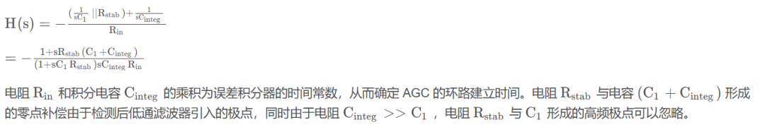
A typical AGC loop generally includes two filters: the first low-pass filter follows the detector to filter out RF transient signals to obtain the amplitude information of the RF signal, while the other low-pass filter and the error amplifier together form an error integration circuit to produce the final gain control signal. The loop filter in this section refers to the error integration circuit in the loop, while the first filter can be considered part of the amplitude detector.
AGC Loop Filter Structure
The bandwidth and time constant of the loop filter determine the establishment time of the loop. Based on specific modulation information and loop steady-state errors, the bandwidth and gain of the loop filter can be determined; therefore, in specific situations, the bandwidth of the loop filter is generally a fixed value. For example, in the W-CDMA receiving system, the AGC loop bandwidth is generally required to be around 200Hz for steady-state output signal errors within ±0.25dB. A typical loop filter structure is shown in the figure above, ignoring the non-ideal effects of operational amplifiers, and the transfer function of the loop filter is represented as:
1. Gain Control Range and Control Characteristics
The gain control range mainly depends on the gain variation range of the VGA in the AGC circuit or the attenuation dynamic range of the VVA, while the gain control range of the overall circuit is determined by the gain/attenuation devices in the circuit, and the reference voltage determines the output level of the automatic gain control. To achieve a constant loop establishment time, the AGC must have a dB linear gain control characteristic.
The common types of variable gain amplifiers used in AGC circuits are analog controlled continuous variable gain VGA or continuous variable attenuation VVA. Another type of variable gain amplifier has its gain controlled by digital quantities, known as Programmable Gain Amplifiers (PGA). Similarly, another type of variable attenuator has its attenuation controlled by digital quantities, known as digital controlled attenuators. For PGAs, gain step size and gain accuracy are two important indicators of gain control characteristics. The gain step size refers to the gain change caused by each LSB gain control word, measured in dB/LSB. Gain accuracy refers to the mismatch between the actual gain and the ideal gain. For PGAs that achieve gain changes through switch toggling, their gain changes are discontinuous, leading to discontinuities in the output signal phase. The same issue exists for digital controlled attenuators, which may also experience discontinuities in attenuation changes. In some phase modulation systems, such phase discontinuities can lead to signal distortion and data loss.
2. Noise Figure
For AGC circuits, as the gain of the circuit varies within a certain range, it is usually not possible to directly measure the noise figure of the AGC circuit. If testing is needed, the AGC circuit can be set to an open-loop state. Additionally, the noise figure of the circuit is inversely proportional to the gain, so it has the minimum noise figure when set to maximum gain.
3. Linearity
Conventional indicators of RF devices typically focus on the 1dB compression point, OIP3, and so on.
4. Port Matching
This specifically refers to circuits using VGA, where the port impedance may not be the conventional 50Ω of RF circuits due to design considerations for bandwidth expansion and noise improvement, necessitating additional matching networks.
4. AGC Circuit Loop Design
For conventional engineering applications, LNA, VGA, VVA, fixed attenuators, and detectors are readily available products, while the design focuses on the negative feedback circuit, i.e., the loop filter/error integrator.
The feedback loop structure of the AGC has been described earlier. A typical AGC loop generally includes two filters: the first low-pass filter follows the detector to filter out RF transient signals to obtain the amplitude information of the RF signal, while the other low-pass filter and the error amplifier together form an error integration circuit to produce the final gain control signal. The first low-pass filter can be considered part of the detector.
With sufficient device margins, the detected voltage can be advanced to a level of operational amplification for following, followed by integration and comparison. This loop filter is similar to the active loop commonly used in phase-locked loops (PLLs), and the ADI phase-locked loop simulation tool SimPLL can be used for quick simulation of loop-related parameters.
5. AGC Circuit Spurious Analysis
The high gain characteristics of AGC circuits, when connected to operational amplifiers, can easily introduce various spurious signals.
1. AGC Spurious Analysis
Common circuit anomalies include high-frequency self-excitation of RF amplifiers or overshooting due to improper selection of control loop parameters, leading to oscillation in the control loop. These issues manifest as unstable or uncontrolled output signals. In AGC circuits with two stages of high-gain RF amplifiers, the spurious issue typically encountered is self-excitation of the RF amplifier. However, the spurious signals generated during this time are usually of high frequency and often occur under small input signal conditions, i.e., under the maximum gain operating conditions.
Appropriate adjustments to loop parameters and adding pre-selection filters can effectively resolve these issues.
There are also instances of low-frequency spurious signals in the output, where spurious signals modulated appear on either side of the main signal, with frequencies differing from the main signal by tens of thousands of hertz. As the signal continues to change, the frequency spacing between the spurious and the main signal also varies slightly, indicating that the signal is correlated with the circuit itself and not an external interference signal.
At this point, monitoring the output voltage of the integrative amplifier circuit reveals that the control voltage has transitioned from a stable DC output to an oscillating signal of several kilohertz, indicating that the spurious signals are generated by the integrative amplifier circuit, entering the RF path through the control end of the variable attenuator and being modulated to appear on either side of the main signal.
Like RF amplifiers, feedback operational amplifier circuits also experience self-excitation issues. It is crucial to consider the amplitude and phase of the feedback signal introduced at the input of the operational amplifier; otherwise, this signal may add positively to the input signal, causing oscillation at the output and transforming the circuit into an oscillator instead of an amplifier.
Methods to assess operational amplifier stability typically employ phase margin and gain margin, with phase margin being more common. Phase margin is defined as the absolute difference between the gain at which the open-loop gain and frequency curve intersects at 180° phase shift and the gain at which the open-loop gain drops to 1. To avoid oscillation and ensure stable operation of the system, it is necessary to minimize the total phase shift when the loop gain equals 1. Generally, the larger the phase margin, the more stable the amplifier. This article employs simulation methods to analyze the phase margin of the operational amplifier circuit, assessing the impact of various components on the stability of the operational amplifier circuit to identify critical factors affecting its stability. Theoretically, when the phase margin is less than 30°, the operational amplifier becomes unstable, with a risk of self-excitation oscillation.
The most significant impact on stability is observed with larger capacitance values, which also leads to the primary cause of spurious issues. The attenuator, as a load for the operational amplifier, also affects stability; the larger the attenuation, the worse the stability.
This can be viewed as a capacitive load for the operational amplifier; from a mechanism perspective, the capacitive load of the operational amplifier and the open-loop output resistance form a pole, whose -20dB per decade slope and 90° phase lag, combined with the -20dB per decade slope and 90° phase lag induced by the operational amplifier itself, lead to a rate close to -40dB, making instability more likely.
2. AGC Spurious Handling
To address the stability impact of the capacitive load in the variable attenuator, improvements to enhance the stability of the operational amplifier circuit can be made in two directions: 1. Reducing the capacitive load; 2. Increasing the operational amplifier’s ability to drive capacitive loads.
In the variable attenuator, the decoupling capacitor C_L serves to filter the ripple from the operational amplifier output and suppress the low-end gain of the RF amplifier, ensuring the stability of the RF amplifier circuit. It cannot be arbitrarily reduced; otherwise, there is a risk of exceeding other indicators and deteriorating the stability of the RF circuit. While retaining this capacitor, the capacitance value can be appropriately reduced according to the actual circuit specifications. To enhance the operational amplifier’s driving capability for capacitive loads, both internal and external compensation methods can be used.
Internal compensation involves connecting a feedback capacitor in parallel with the feedback resistor of the operational amplifier; the basic principle is to achieve phase lead compensation. This compensation method can affect the integration speed of the operational amplifier, thereby altering the response time of the AGC circuit, making this compensation method not widely applicable.
External compensation involves connecting a resistor in series at the output of the operational amplifier, followed by the next stage; the resistance value can range from a few to several tens of ohms, depending on the capacitance of the subsequent stage. This scheme is commonly used to solve instability caused by capacitive loads, with the basic mechanism being that under capacitive load conditions, the loop gain decreases under the influence of C_L. Simultaneously, the phase and gain are no longer proportionally related, and phase lag becomes the determining factor, causing the feedback loop to lose stability, potentially leading to oscillation in extreme cases. By connecting a small resistor R at the output of the operational amplifier, phase lag caused by C_L can be eliminated. Additionally, a resistor can be connected in series with the detector output voltage, primarily for current limiting protection and to reduce the impact of noise and spurious on the control voltage. From a circuit principle perspective, the input of the operational amplifier is high impedance, so increasing this resistor value does not adversely affect circuit performance.
Future Perspectives
Low-frequency AGC circuits can be implemented with a single chip, while higher frequencies require discrete components. Using VGA chips simplifies circuit implementation, whereas using VVA chips complicates the circuit due to most RF VVA chips often requiring dual negative voltages for control, necessitating additional voltage conversion chips and operational amplifiers. Therefore, miniaturization of AGC design remains a challenging aspect.
Note: The views expressed in this article solely represent the author’s opinion, and no guarantees or commitments are made regarding the content. Readers should reference and verify its authenticity and legality. If you find any errors in the source attribution of images, texts, or videos, or if your rights are infringed, please inform this public account, and we will promptly modify or delete it.