“ Memory mapping is the design in which the MCU assigns unique addresses to memory and peripheral registers, similar to assigning house numbers to resources, allowing the CPU to interact precisely. It is divided into unified addressing (shared address space) and independent addressing (address isolation). Modern architectures focus on unified addressing, complemented by enhanced mechanisms such as page mapping and bit-banding operations, balancing efficiency and complexity.。”

01
—
What is “Memory Mapping”?
The core of the MCU is the CPU, which needs to interact with various “resources” to function. These resources include:
Memory:
Such as RAM (Random Access Memory, used for temporary data storage), ROM/Flash (Read-Only Memory, used for storing program code or constants);
Peripheral Registers:
Such as configuration registers for GPIO (General Purpose Input/Output), baud rate registers for UART (Universal Asynchronous Receiver-Transmitter), and count registers for timers (peripherals receive control commands or feedback status from the CPU through registers).
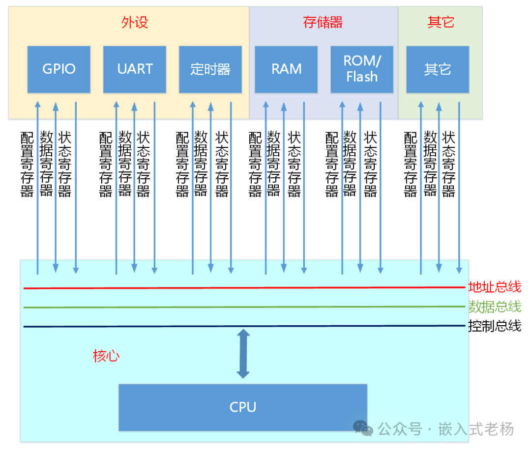
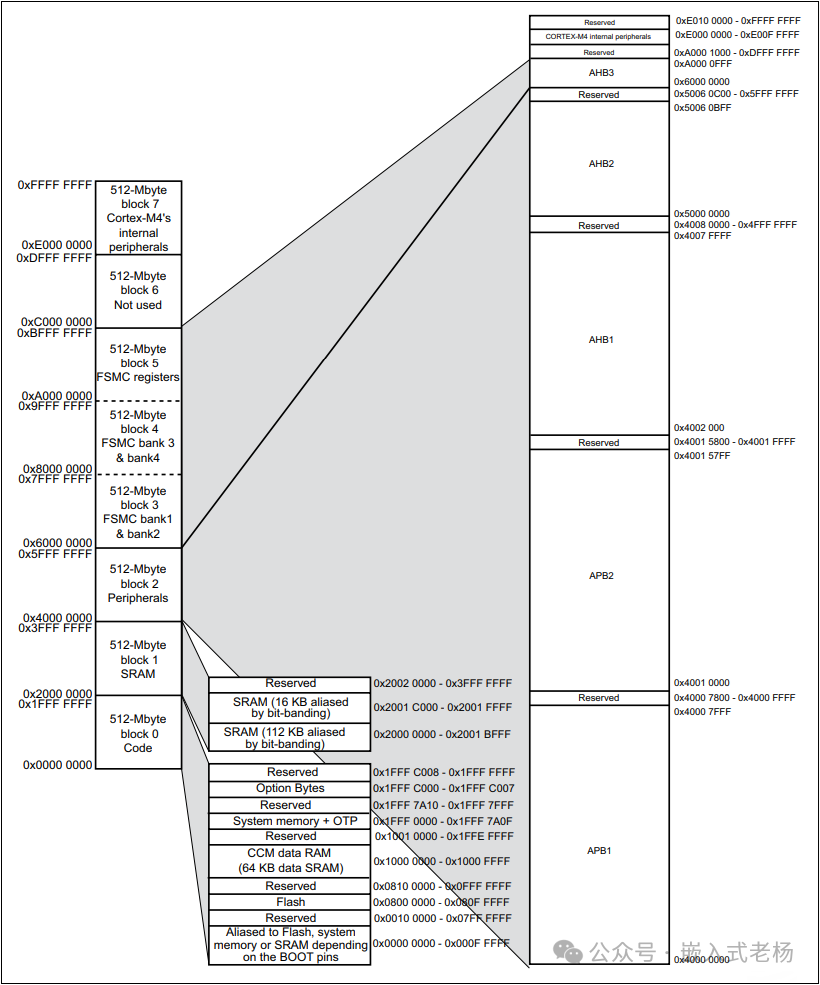
“Memory mapping” is the process in MCU hardware design that assigns unique physical addresses to these resources—just like assigning house numbers to each room, allowing the CPU to find the corresponding resources and perform read and write operations through “addresses.” Ultimately, all resources accessible by the CPU (memory, peripheral registers) will be mapped to a continuous address space, forming a “memory mapping table” (often labeled as “Memory Map” in manuals).
02
—
Basic Addressing Model
The basic addressing model determines the address management rules for memory and peripherals, serving as the underlying constraint of MCU architecture design. Different architectures derive differentiated implementations due to hardware characteristics.
1. Unified Addressing (Memory-Mapped I/O, MMIO)
Memory (Flash/RAM) and peripheral registers share the same logical address space, distinguishing resource types through address ranges, allowing the CPU to access all resources using standard memory instructions.
ARM Cortex-M (STM32F103): 32-bit address space specification divides, with peripherals mapped starting from 0x40000000.
#define GPIOA_BASE 0x40010800  // Base address of GPIOA
#define GPIOA_CRL (*(volatile uint32_t*)(GPIOA_BASE + 0x00))  // Configuration register
#define GPIOA_ODR (*(volatile uint32_t*)(GPIOA_BASE + 0x0C))  // Output register
void GPIOA_Init() {
    GPIOA_CRL = 0x00000003;  // PA0 push-pull output
    GPIOA_ODR |= (1 << 0);   // Set PA0 high
}
RISC-V (GD32VF103): Compatible with Cortex-M address layout, instruction set differences do not affect mapping logic.
#define GPIOC_BASE 0x40011000  // Base address of GPIOC
#define GPIOC_CTL0 (*(volatile uint32_t*)(GPIOC_BASE + 0x00))  // Control register
#define GPIOC_ODR (*(volatile uint32_t*)(GPIOC_BASE + 0x0C))   // Output register
void GPIOC_Init() {
    GPIOC_CTL0 = 0x00000003;  // PC0 push-pull output
    GPIOC_ODR |= (1 << 0);    // Set PC0 high
}
AVR (ATmega328P, Harvard architecture variant): Physically separated but logically unified, peripheral addresses are fixed.
#define DDRB (*(volatile uint8_t*)0x24)  // Port B direction register (address 0x24)
#define PORTB (*(volatile uint8_t*)0x25) // Port B output register (address 0x25)
void LED_Init() {
    DDRB |= (1 << 5);  // Configure PB5 (Arduino LED) as output
    PORTB |= (1 << 5); // Set PB5 high to light up LED
}
Architecture adaptation characteristics:
|
Architecture |
Address Space Size |
Core Advantages |
Typical Application Scenarios |
|
Cortex-M |
4GB |
Ample addresses, supports DMA/pointer access |
IoT, industrial control |
|
RISC-V |
4GB |
Open-source architecture, compatible with MMIO design |
Edge computing, smart hardware |
|
AVR |
64KB |
Logically unified simplifies programming |
Low-power sensor nodes |
2. Independent Addressing (Port-Mapped I/O, PMIO)
Memory and peripherals use completely independent address spaces, and the CPU must access peripherals through dedicated I/O instructions, with memory instructions only affecting memory space.
8086 Processor: Classic independent addressing, with physical separation of memory and I/O space.
; Memory access: MOV AX, [0x2000]  ; Read data from memory address 0x2000 into AX
; I/O access: IN AL, 0x3F8       ; Read data from serial I/O port 0x3F8 into AL;
;          OUT 0x3F8, AL      ; Write AL data to serial I/O port 0x3F8
Traditional 8051 (e.g., AT89C51): Retains independent I/O space, compatible with old code
// Special Function Registers (SFR) accessed through independent space, require dedicated instructions
sfr P0 = 0x80;  // P0 port register (independent I/O address 0x80)
sfr TMOD = 0x89; // Timer mode register (independent I/O address 0x89)
void IO_Init() {
    P0 = 0xFF;    // Directly write to P0 port (dedicated SFR access mechanism)
    TMOD = 0x01;  // Configure Timer 0 to mode 1
}
Architecture adaptation characteristics
|
Architecture |
I/O Space Size |
Core Advantages |
Typical Application Scenarios |
|
8086 |
64KB |
Address isolation, compatible with early peripherals |
Industrial legacy devices |
|
8051 |
128B (SFR) |
Simplified peripheral control, compatible with old code |
Low-end embedded control |
03
—
Enhanced Mapping Mechanisms
Enhanced mapping mechanisms supplement unified addressing to address issues such as small address space expansion and dynamic scene adaptation. Different architectures implement these mechanisms differently due to hardware capability differences.
1. Page Mapping
Divides large physical memory into “pages,” dynamically switching active pages through page registers to overcome hardware limitations of address lines.
PIC16F877A (8-bit Harvard architecture): Program memory paged access
#define PCLATH (*(volatile uint8_t*)0x0A)  // Program counter high byte register
#define PAGE_SIZE 0x400  // Each page 1KB (0x000~0x3FF)
void JumpToPage(uint8_t page, uint16_t offset) {
    PCLATH = (page << 3);  // Set page high byte (each page occupies 3 address bits)
    ((void(*)(void))(offset))();  // Jump to target page address
}
AVR (ATmega128): Data memory extended paging
#define XDIV (*(volatile uint8_t*)0x30)  // Extended data page register
#define EXT_MEM_BASE 0x100  // Base address of extended data area
uint8_t ReadExtMem(uint8_t page, uint16_t offset) {
    XDIV = page;  // Select data page
    return *(volatile uint8_t*)(EXT_MEM_BASE + offset);  // Read current page data
}
8051 (STC89C52): Program memory paged extension
#define ISP_CONTR (*(volatile uint8_t*)0xC7)  // ISP control register
#define PAGE_SHIFT 11  // Each page 2KB (2^11=2048)
void PageWrite(uint8_t page, uint16_t addr, uint8_t data) {
    ISP_CONTR = (page << (16 - PAGE_SHIFT)) | 0x80;  // Enable paging
    *(volatile uint8_t*)(addr) = data;  // Write to current page address
}
Architecture adaptation characteristics:
|
Architecture |
Single Page Size |
Maximum Number of Pages |
Core Uses |
|
PIC16 Series |
1KB~4KB |
8~32 Pages |
Program memory expansion |
|
AVR Mega Series |
512B~2KB |
4~8 Pages |
Data memory expansion |
|
Enhanced 8051 |
2KB~8KB |
16~64 Pages |
Memory expansion compatible with old architectures |
2. Dynamic Remapping
Dynamically modifies the mapping relationship between physical storage and logical addresses through register configuration, adapting to multiple operating scenarios.
STM32F4 (Cortex-M4): Interrupt vector table remapping
#define SCB_VTOR (*(volatile uint32_t*)0xE000ED08)  // Vector table offset register
void RemapVectortoRAM() {
    SCB_VTOR = 0x20000000;  // Remap vector table to RAM base address
}
GD32VF103 (RISC-V): Flash code remapping to RAM execution
#define SYSCFG_CFG0 (*(volatile uint32_t*)0x40010000)  // System configuration register
void RemapCodeToRAM() {
    SYSCFG_CFG0 |= (1 << 0);  // Enable code area remapping (0x00000000 points to RAM)
}
Architecture adaptation characteristics:
|
Architecture |
Remapping Range |
Typical Applications |
Implementation Complexity |
|
Cortex-M |
Vector table / Code area |
Online firmware updates |
Low (standardized registers) |
|
RISC-V |
Code area / Peripherals |
Performance optimization (RAM execution) |
Medium (vendor-specific registers) |
3. Bit-Banding
Maps individual bits of registers to separate alias addresses, allowing atomic operations on single bits through access to alias addresses, supported by only some architectures.
ARM Cortex-M3/M4 (STM32L431): Peripheral and memory bit-banding regions
#define PERIPH_BB_BASE 0x42000000  // Base address of peripheral bit-banding alias region
#define GPIOB_ODR_ADDR 0x40010C0C  // GPIOB output register address
// Bit-banding address calculation macro
#define BITBAND_PERIPH(addr, bit) (PERIPH_BB_BASE + ((addr - 0x40000000) << 5) + (bit << 2))
void SetBitAtomic() {
    // Atomically set bit 5 of GPIOB without affecting other bits
    *(volatile uint32_t*)BITBAND_PERIPH(GPIOB_ODR_ADDR, 5) = 1;
}
Architecture adaptation characteristics
|
Architecture |
Support Status |
Bit-Banding Region Size |
Core Advantages |
|
Cortex-M3/M4 |
Fully supported |
Peripheral 1MB→32MB alias region |
Atomic operations, no side effects |
|
AVR/RISC-V |
Not supported |
– |
Must use masking operations instead |
04
—
Summary of Multi-Architecture Mapping Features
|
Mapping Type |
Core Features |
Supported Architectures |
Typical Instructions/Registers |
|
Unified Addressing |
Shared address space, accessed by standard instructions |
All modern architectures (Cortex-M/AVR/RISC-V) |
LDR/STR/MOV |
|
Independent Addressing |
Address isolation, dedicated I/O instructions |
8086/Traditional 8051 |
IN/OUT/SFR direct access |
|
Page Mapping |
Paging expands address space |
PIC/AVR/Enhanced 8051 |
PCLATH/XDIV/ISP_CONTR |
|
Dynamic Remapping |
Dynamically adjusts mapping relationships |
Cortex-M/RISC-V |
SCB_VTOR/SYSCFG_CFG0 |
|
Bit-Banding |
Bit-level alias atomic operations |
Cortex-M3/M4/M7 |
Bit-banding alias address access |
Modern mainstream architectures (Cortex-M/RISC-V) focus on unified addressing, enhanced by dynamic remapping and bit-banding operations for flexibility, adapting to complex scenarios; traditional 8-bit architectures (AVR/PIC/8051) are limited by address space, relying on page mapping to expand memory while retaining some independent addressing for compatibility with old code; during development, it is essential to prioritize the native mapping features of the architecture (such as bit-banding in Cortex-M and remapping in RISC-V) to balance hardware efficiency and programming complexity.