
Table of Contents
1. Can chips send emails? What is Mailbox?
2. Technical principles and implementation of Mailbox in chips
3. Role in autonomous driving
4. Conclusion

Figure: A typical Mailbox, sourced from the internet
1. Can chips send emails? What is Mailbox?
Modules within a chip do not actually send letters to each other. The term Mailbox borrows the concept of a mailbox at home, where the method is “you put in, I take out; I put in, you take out” to achieve communication between on-chip modules.
In modern integrated circuit design, Mailbox is a critical on-chip communication mechanism that plays a core role in data exchange and collaborative work between processing units. As autonomous driving technology evolves towards higher levels (L4/L5), the computational power requirements of in-vehicle chips are growing exponentially, making multi-core, heterogeneous, and ultra-heterogeneous computing architectures mainstream. The design quality of Mailbox directly affects the system’s real-time performance, reliability, and safety.
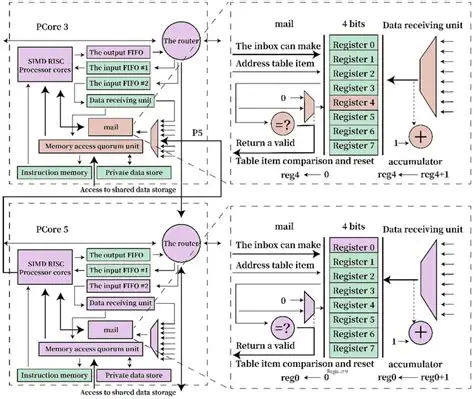
Figure: Data interaction between cores in a chip via Mailbox, sourced from the internet
Mailbox is not only a mechanism but also hardware, which can be imagined as a storage module with a controller. As shown in the figure, the storage space of Mailbox (called the message buffer) consists of multiple registers (which are expensive and originally used only within the Core), and these registers are arranged in a FIFO (First In First Out) queue format.
Its importance is self-evident; ultra-heterogeneous SoC chips used in autonomous driving and intelligent cockpits contain various heterogeneous computing cores, such as CPU, GPU, NPU, ISP, etc. The efficiency of data exchange between them determines the overall performance of the chip.
2. Technical principles and implementation of Mailbox in chips
Mailbox originated from the inter-process communication needs of early multiprocessor systems. In single-chip systems, it achieves asynchronous data exchange between different processing units (CPU cores, GPU, DSP, dedicated accelerators, etc.) through hardware logic. Essentially, it is a hardware module that includes a storage buffer, control registers, and interrupt logic.
Modern autonomous driving chips generally adopt a “CPU+GPU+ASIC” heterogeneous architecture to meet the computational power requirements of different tasks such as perception, decision-making, and control, thus requiring Mailbox for inter-core data exchange.
2.1 Basic structural components
A typical Mailbox module consists of the following core components:
Message buffer: Used to store data frames to be transmitted, supporting fixed-length or variable-length messages, usually adopting a FIFO (First In First Out) queue structure to ensure data order.
Control register group: Includes status registers (indicating buffer empty/full status), configuration registers (setting interrupt trigger conditions), address registers (specifying message source/destination addresses), etc.
Interrupt controller: Notifies the target processing unit through interrupt signals when a message arrives or is sent, avoiding ineffective polling operations.
Arbitration logic: In multi-master device access scenarios, resolves bus conflicts through a priority mechanism, ensuring timely transmission of high-priority messages.
Mailbox communication typically includes the following steps (taking ARM and DSP communication as an example):
1. Initialize shared memory: Allocate a memory area accessible by both parties
2. Configure Mailbox registers: Set interrupt trigger methods and message queues
3. Send message: Write data to shared memory, trigger Mailbox interrupt
4. Receive processing: The receiver reads shared memory data through interrupts
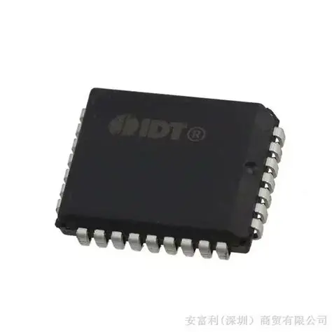 Figure: Independent FIFO memory (model IC FIFO 4KX9 15NS 32PLCC), sourced from the internet
The internal Mailbox packaging is quite deep, and the FIFO cache is just one component of Mailbox, making it harder to find physical illustrations. Therefore, this article uses the above independent FIFO memory to visualize.
The FIFO cache of Mailbox uses the fastest and most expensive storage unit: registers, which are originally used in the processor’s internal highest-speed devices to cache intermediate computation results. A cheaper Mailbox FIFO cache might use L1 or L2 level caches, but almost no Mailbox uses memory as a cache because it is too slow.
|
Features |
Register |
Cache |
Main Memory |
|
Physical Location |
Integrated within the CPU |
Located within the CPU chip (L1/L2) or external (L3) |
Independent chip from the CPU (e.g., DRAM module) |
|
Material |
Flip-Flop |
SRAM (Static Random Access Memory) |
DRAM (Dynamic Random Access Memory) |
|
Speed |
Fastest (nanosecond level, about 0.1-1ns) |
Faster (about 1-10ns) |
Slower (about 50-100ns) |
|
Capacity |
Very small (usually only dozens to hundreds in CPU cores, total capacity in KB) |
Medium (MB level, e.g., L3 cache can reach 64MB) |
Larger (GB level, commonly 8-64GB) |
|
Cost |
Extremely high (cost per GB is thousands of times that of memory) |
Higher (cost per GB is 10-100 times that of memory) |
Lower |
|
Power Dependency |
No refresh needed (data lost immediately on power off) |
No refresh needed (data lost immediately on power off) |
Needs periodic refresh (otherwise data is lost) |
2.2 Not every SoC chip has a Mailbox; one SoC can have many Mailboxes
Mailbox is mainly used to implement communication between multi-core or multi-processing units within SoC chips. Some heterogeneous multi-core SoCs typically integrate Mailbox modules. For example, Texas Instruments’ TDA4VM has multiple different types of cores, and its hardware provides a Mailbox hardware module for inter-core communication. Rockchip’s RK3576S SoC supports one 14-channel Mailbox for communication services between CPU and MCU. ARM’s PL320 is also a Mailbox hardware module designed specifically for inter-core communication.
However, some simpler or more singularly architected SoC chips may not have a Mailbox. For instance, the Semidrive E3106 chip lacks a Mailbox due to resource constraints, necessitating the removal of Mailbox-related folders in relevant projects. The UM2082F08 is an ultra-low-power SoC chip based on a single-cycle 8051 core, which integrates various peripheral communication interfaces but does not mention a Mailbox module. The PHY6235 is a SoC for Bluetooth low energy applications, equipped with SRAM, ROM, and radio, but similarly lacks any description of a Mailbox.
With the development of chip technology, especially the widespread application of multi-core heterogeneous chips, the number of processing units within chips is increasing. To achieve efficient inter-core communication, multiple Mailboxes are needed to meet the communication needs between different processing units. For example, ARM’s PL320 chip supports a total of 32 Mailboxes, each containing 7 data registers, capable of sending up to 28 bytes of data at once. Texas Instruments’ TDA4VM chip’s MAILBOX0 is integrated within the NAVSS0 domain, containing 12 mailbox entities, each of which can be used as a separate mailbox peripheral and can generate 4 interrupt numbers with different interrupts, enabling inter-core communication among 4 cores.
Texas Instruments’ J721E SoC has 12 hardware mailbox instances, each with 16 FIFO queues, totaling 12×16 hardware mailbox queues.
Hardware mailbox instances are independent hardware mailbox modules within the J721E SoC, each of which can be used for communication between different processing units (such as CPU cores, accelerators, etc.). These instances serve as independent communication channels, capable of processing different message-passing tasks in parallel, helping to improve the system’s communication efficiency and flexibility. For example, one hardware mailbox instance can be used to transmit sensor data, while another can be used to send control commands.
Each hardware mailbox instance contains 16 unidirectional hardware mailbox queues. These queues are essentially FIFO (First In First Out) queues used to store and manage messages in order. Each queue can connect to 4 communication users or CPUs. For instance, when one CPU needs to send multiple messages to another CPU, these messages can sequentially enter one of the 16 queues, and the receiving CPU reads messages from the queue in a first-in-first-out order, ensuring ordered message transmission.
Taking the Nvidia Drive Orin chip as an example, its Mailbox system adopts a distributed architecture, with each computing cluster (GPC, TPC, DLA) equipped with an independent Mailbox controller, enabling cross-cluster communication via the on-chip network (NoC), supporting a maximum message transmission bandwidth of 4GB/s.
2.3 Functionally safe Mailbox design
Autonomous driving chips must meet the ISO 26262 functional safety standard (highest ASIL-D level). As a key communication component, the safety mechanisms of Mailbox include:
Message verification: Detect transmission errors through CRC (Cyclic Redundancy Check) or ECC (Error Correction Code) to ensure data integrity
Timeout monitoring: Set a message transmission timeout threshold, triggering safety mechanisms (such as retries or downgrades) if the threshold is exceeded
Redundant channels: Critical control signals are transmitted via dual Mailbox channels, with consistency checks to identify potential faults
Isolation mechanisms: Achieve communication isolation between different security domains through hardware firewalls, preventing fault propagation
The Mailbox system of Texas Instruments’ TDA4VM chip adopts a “dual-port + lock-step core” design, where each message is simultaneously sent to two independent buffers during transmission, verified for consistency by lock-step CPUs to ensure the safety of the transmission process.
2.4 Mailbox in heterogeneous SoCs can be controlled programmatically
As a chip user (rather than a developer), programming operations on the Mailbox within the chip are necessary in the following typical scenarios:
1. System function expansion and customization development
Scenario: When using off-the-shelf chip modules (such as industrial control modules, in-vehicle ECUs), custom functions need to be implemented through Mailbox
Example:
On the TI Sitara AM62x processor, configure the DSP core to run custom algorithms (such as motor control) via Mailbox
Modify the Mailbox interrupt priority of the NXP i.MX8MP to optimize real-time response (such as robotic joint control)
2. Multi-OS collaboration
Scenario: Coordinating resources when the chip runs heterogeneous OS (such as Linux + RTOS)
Operation example:
Send urgent sensor events (such as temperature exceeding limits) to the RTOS core via Mailbox registers
Configure shared memory addresses between RISC-V core and ARM core on the Allwinner D1 chip
3. Peripheral driver development
Scenario: Writing drivers for third-party IP cores (such as AI accelerators)
Technical points:
Set Mailbox command codes (e.g., 0x01 to start inference, 0x02 to read results)
Handle timeout retransmission mechanisms (e.g., CAN FD controller Mailbox’s 500ms timeout setting)
4. Fault diagnosis and recovery
Scenario: Obtaining co-processor status via Mailbox during system anomalies
Practical methods:
Read the Mailbox status register to determine if the DSP is unresponsive (e.g., MBX_STAT register of ST STM32MP157)
Send watchdog reset commands via the safe Mailbox channel
5. Performance tuning
Scenario: Optimizing multi-core task scheduling delays
Typical operations:
Adjust Mailbox interrupt trigger methods (edge/level triggered)
Allocate dedicated Mailbox channels for high-priority tasks (e.g., COM layer in automotive Autosar architecture)
The typical process for users operating the Mailbox is illustrated in the following diagram
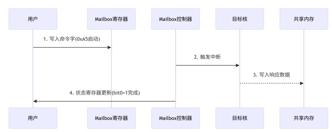
Figure: Typical flowchart for operating Mailbox
Note that debugging hardware registers for the Mailbox controller relies on physical address mapping, requiring access to real hardware registers via development boards; or during multi-core communication validation, actual hardware verification of inter-core interrupt triggering and message passing functions (such as ARM and DSP communication) also requires chip development boards.
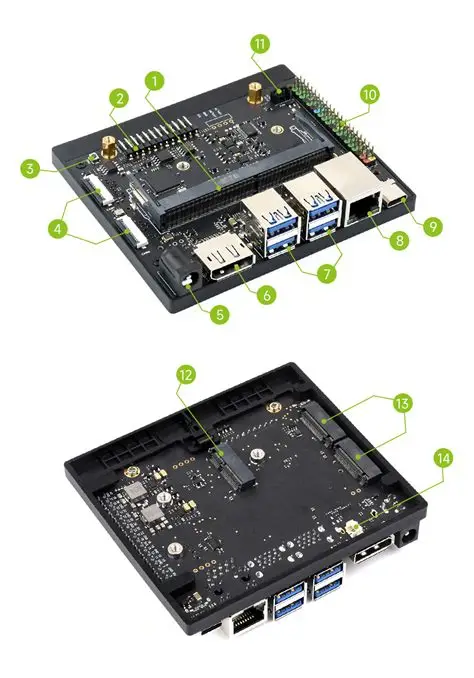
Figure: Front and back of the Orin chip development board, sourced from the internet
Typical code example: ARM core sending data to DSP core (TI AM57xx platform)
// ARM core sender code
void arm_send_to_dsp(uint32_t *data, uint32_t size) {
// 1. Write to shared memory
memcpy(SHARED_MEM_ADDR, data, size);
// 2. Trigger Mailbox interrupt (write message to Mailbox register)
MAILBOX_REG_WRITE(MAILBOX_DSP_INT, SHARED_MEM_ADDR);
// 3. Wait for DSP acknowledgment (optional)
while (!(MAILBOX_REG_READ(MAILBOX_ARM_ACK) & 0x1));
}
DSP is Digital Signal Processor
3. Role in autonomous driving
The core demand of autonomous driving systems is to achieve safe and reliable decision-making control in complex dynamic environments, which places extremely high requirements on the real-time performance, computational density, and functional safety of in-vehicle chips. As the “neural hub” of heterogeneous computing architecture, the design of Mailbox must meet three core requirements: low-latency communication, deterministic response, and fault isolation.
Low-latency communication
Low-latency requirement: The transmission delay of LiDAR point cloud data must be controlled within 1ms; otherwise, it will lead to temporal offsets in environmental perception, affecting obstacle distance judgment.
Bandwidth bottleneck: An 8-line LiDAR generates about 2 million point cloud data per second, requiring Mailbox to provide at least 16Gbps of transmission bandwidth (each point contains x/y/z/reflection information).
Priority scheduling: The frame synchronization signal of the camera must be set to the highest priority to ensure temporal alignment of multi-sensor data.
When Mailbox bandwidth is insufficient, it can lead to sensor data backlog, causing the perception system to experience “data starvation”. Some autonomous driving test data shows that for every 10ms increase in Mailbox delay, the missed detection rate of obstacles increases by 3.2%, which could lead to severe consequences in high-speed scenarios.
Deterministic response
The transmission delay jitter of emergency braking commands must be less than 100μs; otherwise, it will lead to significant deviations in braking distance.
Fault tolerance: A single point of failure in Mailbox should not result in the loss of control commands, requiring redundant designs to achieve “zero data loss”.
Time synchronization: The decision-making and control units must exchange timestamp information via Mailbox to ensure temporal consistency between control commands and vehicle status.
In autonomous driving systems, Mailbox failures can lead to catastrophic consequences. An accident investigation of an autonomous driving test vehicle in 2022 revealed that due to a defect in the Mailbox interrupt handling logic, braking commands were delayed by 350ms, ultimately causing a rear-end collision. This has prompted the industry to strengthen dual verification of Mailbox hardware diagnostics and software monitoring.
Mailbox deployment in heterogeneous computing environments achieves fault isolation
Common heterogeneous computing SoCs may contain the following computing cores on the same chip (including but not limited to):
CPU clusters: Responsible for system scheduling, logical decision-making, and other serial tasks
GPU/TPU: Handle image recognition, point cloud segmentation, and other parallel computing tasks
ASIC accelerators: Dedicated hardware modules, such as NVIDIA’s DLA (Deep Learning Accelerator), TI’s radar signal processors, etc.
Mailbox forms a multi-level communication network in such architectures:
Internal Mailbox: Communication between different cores within the same computing unit, such as message passing between CPU cores, with delays typically within 100ns.
Cross-domain Mailbox: Connects different computing units, such as communication between CPU and GPU, achieved through on-chip networks, with delays of about 1-5μs.
External Mailbox: Communication interface between the chip and external devices, such as interaction with CAN controllers and Ethernet PHY, with delays significantly influenced by external buses.
Moreover, external or cross-domain Mailboxes may have hardware-level encryption, integrating AES-GCM and other encryption engines to perform real-time encryption and decryption of sensitive messages (such as control commands);
and intrusion detection, which analyzes Mailbox communication patterns to identify abnormal traffic, promptly detecting potential network attacks; as well as security island design, which partitions independent security zones within Mailbox for transmitting ASIL-D level critical messages.
These measures further implement fault isolation functionality.
For example, Tesla’s FSD chip employs two independent computing clusters (each containing 12 CPU cores + neural network accelerators), with inter-cluster communication achieved through dedicated Mailbox channels, ensuring that basic system functions can be maintained even in the event of a single cluster failure.
4. Conclusion
As autonomous driving technology advances towards level L4, the Mailbox system faces multiple challenges, including surging bandwidth demands, tightening latency constraints, and heightened safety requirements, with its technological evolution presenting three major trends:
Traditional Mailbox bandwidth allocation and priority settings are mostly statically configured, making it difficult to adapt to the complex and variable driving scenarios. The next generation of Mailbox will introduce adaptive scheduling mechanisms:
Scenario-aware scheduling: Automatically adjust message priority based on real-time road conditions (such as congestion, high speed, intersections), for example, increasing the transmission priority of camera data in intersection scenarios.
Predictive pre-allocation: Use machine learning to predict short-term communication needs, reserving bandwidth resources in advance for high-priority tasks.
Load balancing: Dynamically allocate traffic among multiple Mailbox channels to avoid single-point congestion.
NVIDIA’s new Drive Thor chip adopts a “smart Mailbox” architecture, achieving dynamic bandwidth management through dedicated communication processors, reducing communication latency by 40% compared to the previous generation, with bandwidth utilization exceeding 90%.
Moreover, the integration of safety and information security (i.e., “SecURity”) has become a new direction for Mailbox design. For instance, Infineon’s AURIX TC4x chip’s Mailbox system employs a dual protection mechanism of “security island + encrypted channel,” with its secure communication module passing Common Criteria EAL5+ certification, effectively resisting side-channel attacks and injection attacks.
The third trend involves using Mailbox to assist in time synchronization among multiple sensors and processors, which is particularly important in autonomous driving. It can be used to achieve time synchronization between processes running on multi-core processors, cross-clock domain data synchronization, and as an auxiliary communication mechanism for time synchronization systems.
In multi-core processor chips, Mailbox can be used to synchronize processes running on multiple cores. For example, Texas Instruments’ AM2632 and AM2612 chips implement Mailbox functionality through CTRLMMR registers and support central platform time synchronization (CPTS) TEXAS INSTRUMENTS. Mailbox can send synchronization signals or timestamp information, allowing each core to coordinate work and ensure consistency of the entire system’s state.
It can also synchronize across clock domains. Processing units in different clock domains can transmit data via Mailbox, avoiding the use of explicit handshake signals. For instance, a process in one clock domain writes data to Mailbox, while a process in another clock domain reads data from Mailbox, achieving cross-clock domain data synchronization.
In the current era where computational power equates to productivity, Mailbox, as the “traffic hub” within chips, will increasingly highlight its importance with the proliferation of autonomous driving, becoming one of the key indicators for measuring the performance of in-vehicle chips.