▼Follow our WeChat public account: Hardware Matters▼
Part 01
Introduction
Why are Gerber files so important?
Gerber files, specifically in the RS-274X format, are the internationally accepted standard format in the PCB manufacturing industry. They serve as the “blueprints” for circuit boards, describing the images of each layer of the circuit board, such as traces, pads, and solder masks, using a series of vector coordinate data. No matter how intricate your design is, it ultimately needs to be accurately conveyed to the production equipment of the PCB factory using this “universal language”.
A single incorrect setting, such as missing components, reversed layers, or omitted layers, can lead to production failures. Therefore, mastering the correct and standardized method of exporting Gerber files is an essential skill for every hardware engineer.
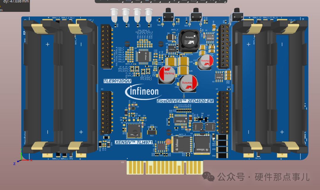
At the end of this article, there will be a way to obtain the BMS schematic + PCB project files, along with Infineon’s examples!
Part 02
Preparation Work
Preparation is crucial; do not skip these key checks before exporting Gerber files. After all, sharpening the axe does not delay the work of chopping wood. It is much simpler to do things correctly the first time than to remedy mistakes afterward. Therefore, before clicking the export Gerber button, please ensure you complete the following critical checks to help you avoid 90% of potential issues.
1. Run DRC one last time
-
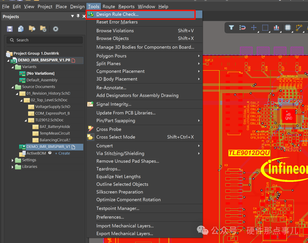
Action: In the PCB editing interface, click the menu bar Tools -> Design Rule Check -> Run Design Rule Check.
-
Purpose: Ensure that your design has no spacing, short circuit, or other violations. Going into production with errors is akin to entering the field with an illness.
2. Confirm and define the board outline
-
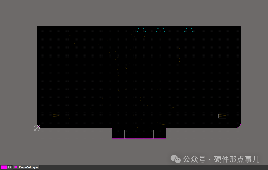
Action: Switch to a dedicated mechanical layer such as Mechanical 1 or Keep-Out Layer, which is set according to personal preference, and ensure you have accurately drawn the closed outline of your circuit board using the line tool (Place -> Line).
-
Purpose: This serves as the basis for the factory to perform cutting (milling). An unclear or unclosed board outline will prevent the factory from determining the final shape of the circuit board.
3. Set the origin
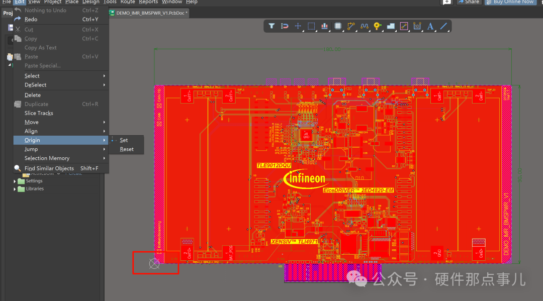
Action: Click the menu bar Edit -> Origin -> Set, then move the mouse to the bottom left corner vertex of the circuit board and click to confirm.
Purpose: To set a unified coordinate origin for your PCB. This helps ensure precise alignment of the Gerber files and subsequent drilling files, reflecting professional practice.
Part 03
Steps to Export Gerber Files
Next are the core operational steps. With the preparation work completed, we officially begin the export process.
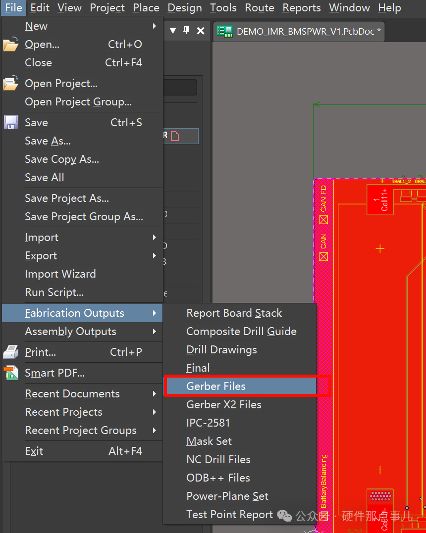
Step 1: Open the Gerber settings window
Path: File -> Fabrication Outputs -> Gerber Files.
Step 2: Configure the “General” tab
This is the most critical step, determining the basic format of the file.
Units: Select Millimeters (mm). Although Inches are also available, my personal preference is mm, as millimeters are a more common and precise standard in modern electronic manufacturing.
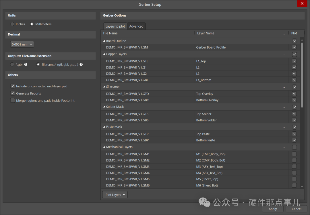
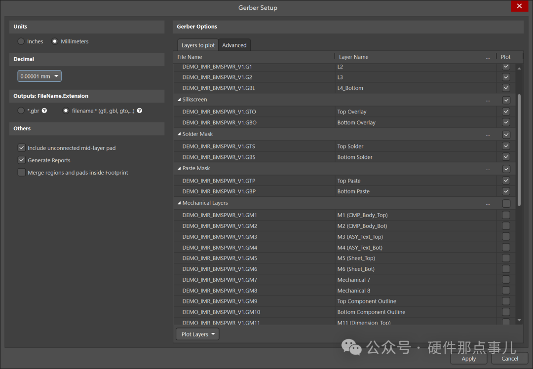
Format/Precision: In older versions of AD, you could select 2:5. This means the integer part has 2 digits, and the decimal part has 5 digits. This is currently the highest precision format, crucial for high-density, fine-line PCBs. Choosing 2:4 or 2:3 may lead to loss of precision, causing pads or traces to deform. Newer versions of AD directly display the precision, such as the 0.00001mm shown below.
Step 3: Configure the “Layers” tab
-
You need to inform the software which layers’ “drawings” need to be printed. Select only the layers you need, and be careful not to select incorrectly, especially the mechanical layers, as this can cause issues!
-
Plot Layers: Click the “Plot All Used Layers” button in the lower right corner to quickly select all used layers, then make adjustments as needed.
-
Mirror: Huge warning, never, ever, ever check the “Mirror” option for any layer! Mirroring should be determined by the CAM engineer of the PCB factory based on their equipment and processes. If you mirror it yourself, there is a high probability that the bottom layer will be reversed, resulting in the circuit board being scrapped. Older versions of AD had this option, but I see that AD23 no longer has it.
-
Standard layers that must be exported:
GTL (Top Layer): Top copper foil
GBL (Bottom Layer): Bottom copper foil
GTS (Top Solder Mask): Top solder mask (green oil)
GBS (Bottom Solder Mask): Bottom solder mask
GTO (Top Overlay): Top silkscreen (white text)
GBO (Bottom Overlay): Bottom silkscreen
G1, G2, … : All intermediate signal layers (if it is a multilayer board)
Keep-Out Layer or Mechanical 1: Your board outline layer, be sure to check this.
Step 4: Configure the “Apertures” tab
Action: Ensure the Embedded Apertures (RS-274X) option is checked.Only older versions of AD require this action!
Purpose: This is the core of the Gerber format, embedding the “brush” shape information (i.e., apertures) of each graphic into the Gerber file, eliminating the need for a separate D-code file. This greatly simplifies the process and reduces the likelihood of errors.
Step 5: Configure the “Advanced” tab
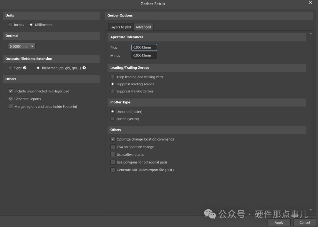
The settings here relate to file compatibility and some detail handling.
Film Size: Keep the default, no need to modify (older versions of AD require this).
Plotter Type: Select Unsorted (Raster). Here, “plotter” actually refers to a photoplotter, a precision device used to convert Gerber data onto film.Unsorted (Raster) is the most recommended option, as the vast majority of PCB manufacturers now use raster photoplotters. Unless your manufacturer explicitly requests the use of Sorted (Vector) format, always use the default Unsorted (Raster).
Key options confirmation:
Gerber File Format: Select RS-274X. This is currently the most universal standard. Gerber X2 is a newer format that includes more data such as stacking information, but not all factories support it. Unless the factory explicitly requests it, using RS-274X is the safest option (older versions of AD require this).
Leading/Trailing Zeros: Select Suppress leading zeros, which is a common practice in the industry.
Step 6: Generate the files
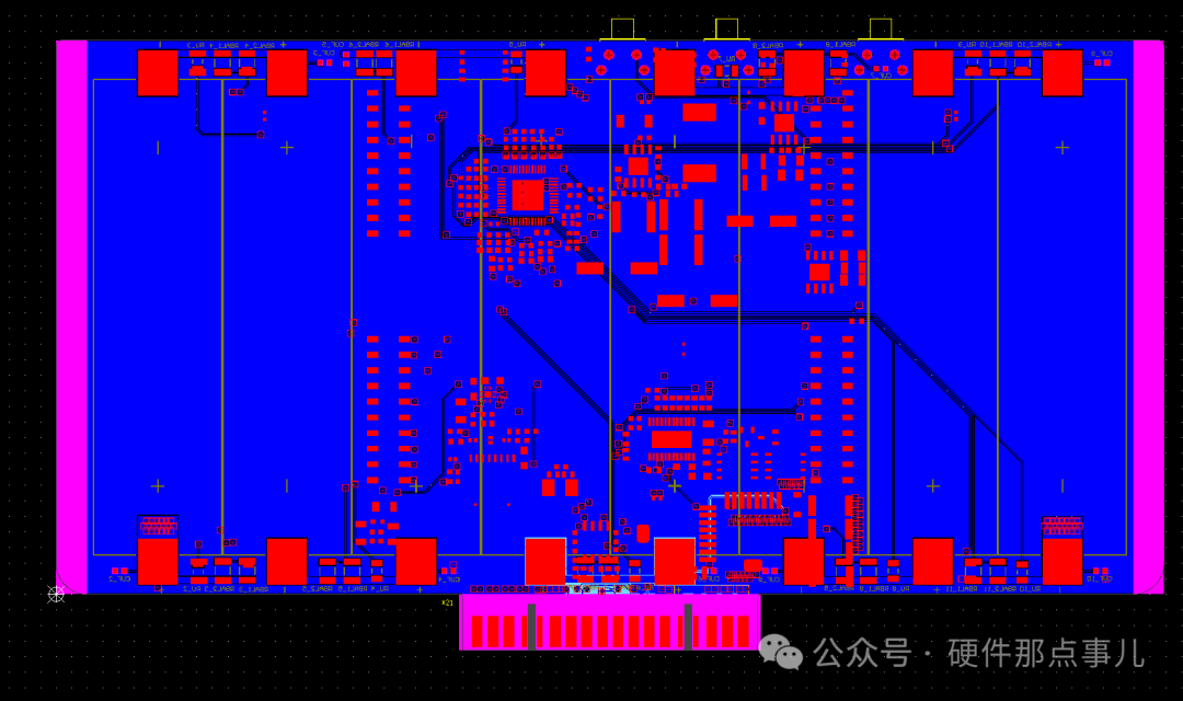
Click OK. AD will automatically generate all the layer files you checked and save them by default in the Project Outputs for [ProjectName] folder within the project folder. At the same time, AD will open a CAMtastic preview window for an initial view of the results.
Part 04
Exporting NC Drill Files
Gerber files only define the graphics, while the drill files (NC Drill File) inform the factory where and how large to drill holes. Both are essential.
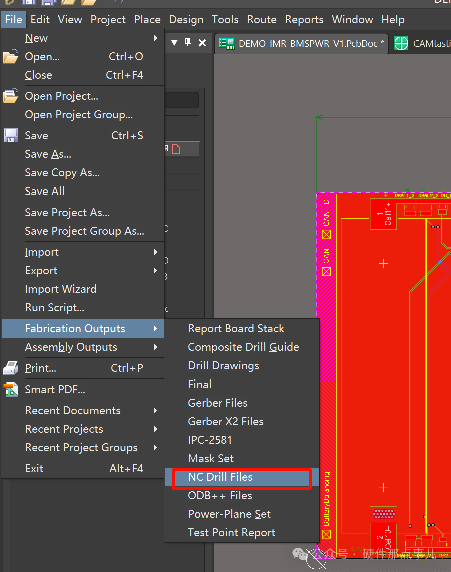
Step 1: Open the NC drill file settings window
Path: File -> Fabrication Outputs -> NC Drill Files.
Step 2: Configure the drill file parameters
The core key: The Units and Format/Precision settings here must be absolutely consistent with the previous Gerber settings! If Gerber is in mm and 2:5, this must also be mm and 2:5. Inconsistency will lead to misalignment of drill positions, resulting in 100% scrapping of the circuit board.
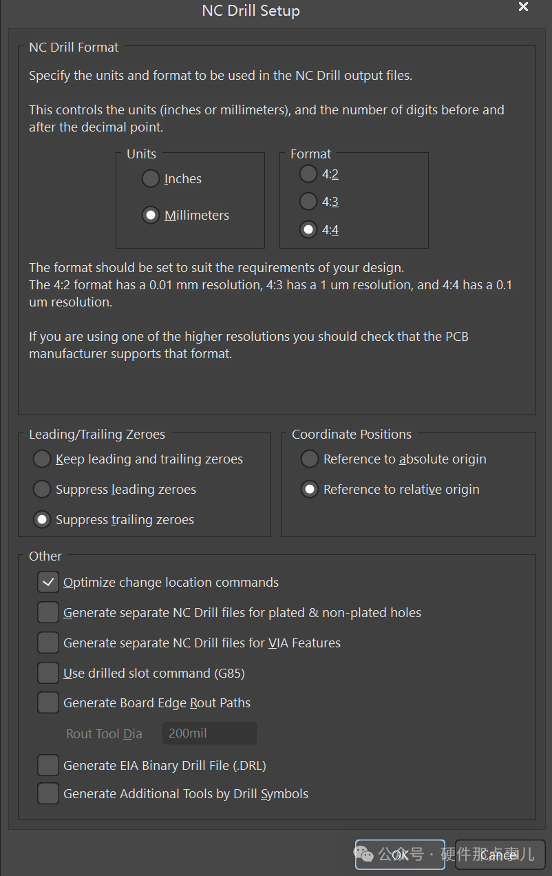
Leading/Trailing Zeros: Similarly, maintain consistency with the Gerber settings by selecting Suppress leading zeros.
Coordinate Positions: Select Reference to absolute origin.
Step 3: Generate the files
Click OK. In the pop-up Import Drill Data dialog, click OK again.
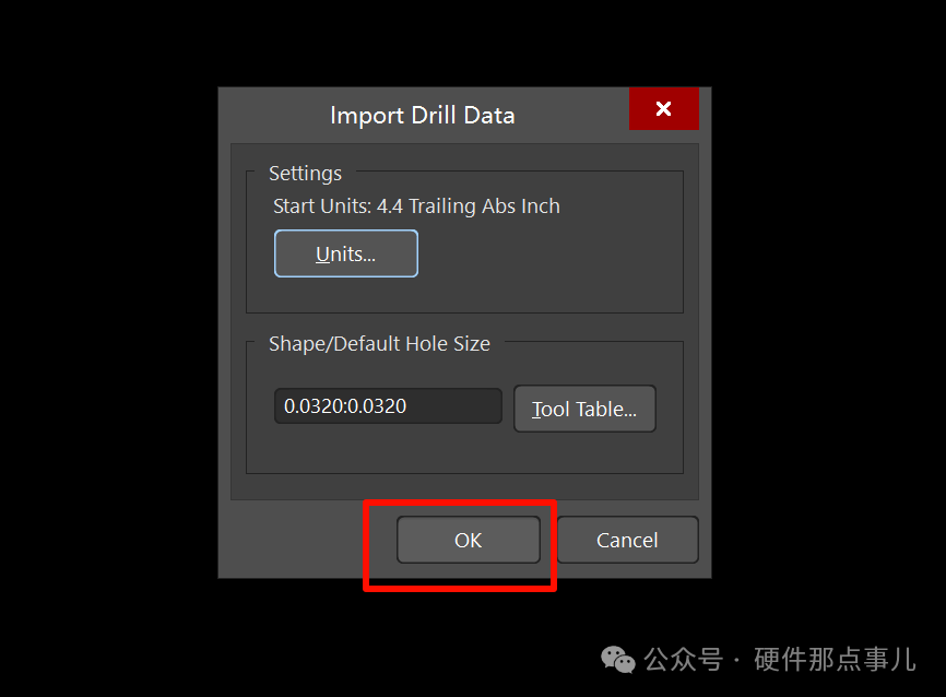
The drill file (usually in .TXT or .DRL format) will be generated in the same output folder as the Gerber files.
Part 05
Review and Packaging
Do not send the files directly to the factory! Please make sure to do the final review yourself.
Use a Gerber Viewer for verification, download a free Gerber viewing software, or use the online viewers provided by many PCB manufacturers (such as JLCPCB, etc.). There are also some excellent DFM software available.
Action: Import all the generated Gerber files (.GTL, .GBL, etc.) and drill files (.TXT) into the viewer at once.
Check the following:
Do all layers align perfectly?
Is the board outline clear and closed?
Are the drill positions correct?
Is the top silkscreen printed on the pads?
Do the dimensions match the design?
Finally, package the files
Select all Gerber files (.GBL, .GTL, .GBO, .GTO, .GBS, .GTS, board outline files, etc.) and NC drill files (.TXT) from the output folder and compress them into a .zip file.
Exporting Gerber files may seem tedious, but it is essentially a meticulous and detailed task. Remember a few core principles: DRC first, unified origin, format precision 2:5 (mm), never mirror, drill file settings consistent with Gerber, and always verify with a third-party viewer.
As long as you strictly follow this process, you can ensure that your hard work in design can be perfectly replicated into a physical circuit board. Let’s all do our best!
Reply with the keyword: BMS in the public account to obtain the BMS schematic + PCB project!

If you have any questions, feel free to leave a comment for discussion!