It is understood that Winbond Electronics is expanding its production capacity, with the new factory located in Kaohsiung, Taiwan, which will be put into production and is expected to produce at a capacity increase of 15-20% annually to meet customer demand. In addition to the layout of production capacity, Winbond Electronics also has representative plans in terms of product technology.

In a recent interview, Winbond Electronics DRAM Product Marketing Manager Tseng Yi-Chun introduced: “In the next year or two, edge computing will become more popular. It is usually believed that AI models are large. However, the industry is working hard to continuously optimize the architecture to shrink AI models, achieving extreme compression while maintaining acceptable accuracy.”

Design Trends of Storage Solutions: External Memory
Driven by emerging technologies such as IoT, artificial intelligence, 5G, big data, and cloud computing, in recent years, the quality of people’s lives has shown a significant rapid iteration. Especially during the COVID-19 pandemic in 2020 and the subsequent post-pandemic era, it has rapidly broadened and activated our new way of life. The rise of short videos has led to an exponential growth of data. Traditionally, this massive data is uploaded to the cloud, where AI technology is used for cloud management, cloud hosting, and cloud mining. However, with the surge of data, the computational load has become too great, facing challenges that are unsustainable. The solution is to transfer the computation directly to the terminal or edge computing.
Indeed, driven by terminal applications and edge computing applications, AI models will continuously optimize towards what is known as compression. Looking across the industry market products, it is not difficult to see this trend change. For example, Google’s most famous TensorFlow Lite for Micro Controllers can reduce the weight size of AI neural model engines to a very low level. There are also manufacturers on the market doing optimization upgrades, such as MobileNetV2-YOLOv3-Nano, which can reduce its weight size to 3.0MB, and even Yolo-Fastest can go down to 1.3MB, with Yolo-Fastest-XL maxing out at 3.5MB.
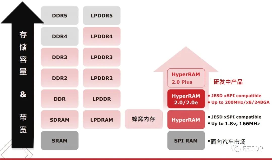
External memory is the future design trend. Currently, major chip manufacturers advocate the HyperBus™ technology when designing memory controllers. This technology was first published by Cypress in 2014. Compared to other memory IC transmission control interfaces, one of the characteristics of the HyperBus™ interface is its low pin count, which simplifies the layout of the circuit board and reduces wiring area. Therefore, Winbond Electronics has also successively launched related HyperRAM™ series products.
It is understood that since the official launch of the HyperRAM new storage product in 2019, Winbond has been able to offer a series of products including HyperRAM1.0, HyperRAM2.0, and HyperRAM2.0e in terms of memory capacity. Among them, the capacity of HyperRAM1.0 is 32Mb; HyperRAM2.0 has a capacity of 64Mb. The 256Mb HyperRAM 2.0/2.0e supports x8 and x16 respectively, achieving a maximum operating frequency of 200MHz under 3.0V or 1.8V working voltage, corresponding to a data transfer rate of 400Mbps.
Key Technologies of HyperRAM
Low power consumption, fewer pins, and ease of design are the main selling points of Winbond’s HyperRAM. For low power consumption, this is actually a major demand for such products in the market. The biggest highlight of Winbond HyperRAM is its ultra-low power consumption. The B/W of HyperRAM 2.0e is about 1GB/s, with a running power consumption of less than 50 microwatts, standby power consumption at room temperature of less than 70 microwatts, and less than 35 microwatts in ultra-low power mode at room temperature.
So how does HyperRAM achieve such low power consumption? It turns out that Winbond has made some special designs in the circuitry. When HyperRAM enters ultra-low power mode, it shuts down all power supplies, retaining only some necessary circuits, while data is continuously stored. Compared to traditional standby modes, the wake-up time of this ultra-low power mode will inevitably be longer. However, Tseng Yi-Chun stated that many IoT devices currently do not require urgent wake-up times, and through communication with customers, it has been found that the wake-up time of HyperRAM in ultra-low power mode is not an issue.
As for the package size, the area of HyperRAM is significantly smaller compared to LPDDR and SDRAM, making it easier to design. In terms of pin count, HyperRAM has very few pins, with currently two types available, 8 I/O and 16 I/O, with 16 I/O being approximately 30 Ball. Compared to traditional LPSDRAM or SDRAM which are 50 or 60 Ball, HyperRAM reduces the pin count by nearly half, with fewer than 30 pins. Therefore, from the user’s perspective, whether in terms of PCB area or design, it will be much simpler, and it can achieve low power consumption without much degradation in bandwidth, meeting current market demands.
Applications of HyperRAM
The application range of HyperRAM is very broad, not only can it be used to store AI data, but it can also be used to store video streams or audio stream data. Currently, the main application market for clients adopting HyperRAM includes 4G feature phones, smartwatches, LTE IoT modules, and AI IoT devices. For example, Winbond’s 64Mb HyperRAM can not only be used to store RTOS but can also be used in simple light intelligence applications, although it cannot perform real-time image recognition. For instance, smart water meters and smart electricity meters typically perform image recognition at a rate of one frame per second, and after that, the data can be transmitted to the central control console via NBIOT. For applications that do not require real-time image parsing, HyperRAM is very suitable.
In addition, it is reported that many small eFPGA companies are using HyperRAM for Display Buffer, requiring a capacity of 32Mb-256Mb. HyperRAM is also used in WiFi IoT devices primarily to provide Data buffer. In fact, WiFi IoT also incorporates some ISP (Image Signal Processing) functions and some MPU, which require higher capacity for image recognition, with a significant starting range from 64Mb to 256Mb.
Tseng Yi-Chun stated that from the end of this year to the beginning of next year, many designs incorporating HyperRAM will be gradually introduced. This includes smart speakers, home cameras, smart doorbells, smart locks, and other smart home applications, as well as industrial human-machine interfaces and even automotive dashboards. It is reported that in Europe, products have already been developed that incorporate HyperRAM into the main unit of electric bicycles.
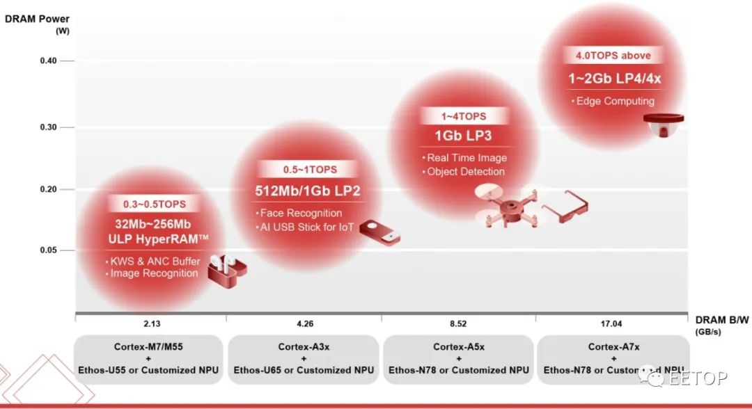
However, overall, the acceptance of HyperRAM among microcontroller and chipset manufacturers will be higher. Tseng Yi-Chun stated that HyperRAM will become increasingly common in new applications that combine microcontrollers and AI, which is also a future development trend. It is reported that based on the current customers cooperating with Winbond, the main microcontrollers paired with HyperRAM are Cortex-M7 or M55, or some other MPU. The applications include KWS (Key Word Spotting) or simple image recognition.
For example, microcontrollers may need to be equipped with RTOS functions, or external WiFi/BT (Bluetooth), or LTE, and even add device-side AI (On Device AI) NPU functions. Under the premise of adding AI functions, using existing SRAM to store RTOS, the space of SRAM is not large enough. Generally, microcontrollers do not configure high-capacity SRAM because the cost is too high. The solution is to adopt external memory processing methods. Currently, mainstream smart devices such as headphones, Bluetooth (Bluetooth), TWS, etc., still mainly use NOR Flash. However, as the demand for derivative applications increases, larger memory is needed to achieve low latency and voice computing functions. Tseng Yi-Chun stated: “External memory is a very good solution. Such products may start appearing on the market next year.”
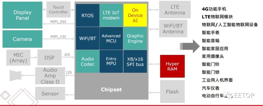
Figure: The application and market of increasing demand for on-device AI in MCU devices for audio/video
In addition to the microcontroller field, Winbond is also actively collaborating with MCU and some system manufacturers to establish the HyperRAM ecosystem. Because the circuit board of the MCU system will not be very large, the required pin count does not need to be too many, so HyperRAM is a very good choice. Tseng Yi-Chun stated that many microcontrollers or industrial control parts currently hope to adopt Winbond HyperRAM. Especially because under low frequency conditions, microcontrollers do not require special DRAM for control; general GPIO at low clock frequencies, such as below 100MHz, can simulate HyperRAM control functions. Therefore, it is very suitable for microcontrollers to adopt HyperRAM products.
Tseng Yi-Chun further shared: “HyperRAM can be used as working memory, suitable for embedded AI and image processing applications in AIoT devices. Winbond continues to conduct research and development and planning for the HyperRAM product line. After 2.0e, there will be 2.0 Plus, which will greatly improve speed again. Next, Winbond will extend the capacity of HyperRAM to 128Mb or even 256Mb, which will allow for more image data or more AI models to be stored. According to Winbond’s expectations, the applications of AIoT will become increasingly widespread in the next two to three years. We hope to launch HyperRAM 3.0 after the market response improves.”
Winbond HyperRAM Plan
NOR+NAND, Fully Enhance AI “Read Speed”
Because currently, AI mostly stores data at the terminal for computation, there are also some AI models that need to be stored at the terminal, usually on NOR Flash or NAND Flash. The usage scenario is to quickly read AI models from flash memory and then transfer them to DRAM/SDRAM or HyperRAM for computation. Therefore, “read speed” has become a very important consideration.
If the AI model is relatively small in capacity, NOR Flash is actually very fast in small capacity reads and is a good choice. However, as more functions are added or the things to be recognized become more complex, the capacity occupied by AI models will become larger. At this time, in large capacity situations, NAND Flash’s read speed is faster than that of NOR Flash. Therefore, in such usage scenarios, it is necessary to choose different capacities of NOR paired with different capacities of NAND to satisfy both small and large capacity fast reads.
Winbond SpiStack: NOR Chip and NAND Chip Stacked Packaging
Winbond SpiStack stacks NOR chips and NAND chips into one package, for example, stacking a 64Mb Serial NOR and a 1Gb QspiNAND chip, allowing designers to flexibly store code in the NOR chip and data in the NAND chip. In addition, although it is a stack of two chips (NOR+NAND), the single package SpiStack only requires 6 signal pins for use.

Two chips become one chip, thus reducing PCB wiring size
In summary, Winbond’s SpiStack has three major advantages: hardware compatibility, cost advantages, and excellent quality. For flash products, customers always expect them to have the following three advantages: small PCB footprint, low cost, and diverse combinations. Winbond’s SpiStack product family can fully meet these demands.
-
First, Winbond combines two different SpiNOR and SpiNAND into one flash product using a standard package. The original NOR is an eight-pin standard package, and the original NAND is also an eight-pin standard package. After being combined, it remains an eight-pin standard package, so there is no need to make any changes in hardware devices, wiring design, or even circuit board design. Because Winbond’s SpiStack package is standard, not a custom package. In addition, the pins of SpiStack correspond completely with the original standard package, so users do not need to redesign the circuit board when using Winbond SpiStack products.
-
The second point is that the selling price of consumer electronics cannot be too high, which requires that the cost of each component must be reduced. The cost is closely related to PCB design. The larger the PCB area, the higher the cost incurred. Winbond’s SpiStack product can stack one NOR Flash with one NAND Flash, reducing the area that would originally require two flash memories to the area of one flash memory, thus reducing the PCB area and allowing users to reduce flash memory costs. The wiring on the circuit board has also changed from originally needing two wires to only needing one wire, further saving PCB area.
-
The third point is that the current product models of Winbond’s SpiStack product line include W25M161AVEIT, W25M321AVEIT, W25M641AVEIT, and W25M121AVEIT, which are NOR Flash of 16Mb, 32Mb, 64Mb, and 128Mb paired with 1Gb NAND. In addition, customers can choose other different capacities of NOR paired with different capacities of NAND. Customers’ considerations have two aspects: one is mainly based on the size of the boot data volume, and the other is to consider the need to store larger data, such as image data or program data. Customers can decide the required NAND Flash and NOR Flash capacity based on these two considerations. Users or system designers will not waste too much cost using flash memory that exceeds the required capacity.
Winbond Electronics Flash Product Marketing Manager Huang Hsin-Wei particularly emphasized that there are also products on the market that combine NOR and NAND chips in one package, but their approach is to switch using physical pins, which cannot maintain the standard pin count of eight and must use a different packaging method. Winbond has introduced a brand new method, using software instructions to switch chips. When it is necessary to control a specific chip, it can be switched using a software method to operate on a specific chip. Each chip has its own identification code, which is pointed to by software. In addition, SpiStack (NOR+NAND) supports concurrent operations, so when one chip is performing write/erase, the other chip can simultaneously perform write/erase/read operations without interference. Thus, SpiStack can also save writing and erasing time. Furthermore, the NAND and NOR used in SpiStack have been verified for automotive-grade quality, and both NAND and NOR are produced using mature processes, so their quality is beyond doubt.
User Case: Renesas RZ/A2M
In early July, Winbond Electronics officially confirmed that Winbond HyperRAM and SpiStack (NOR+NAND) products will be used in conjunction with Renesas’ Arm-based RZ/A2M microprocessor (MPU). The Renesas RZ/A2M belongs to the RZ series of microprocessors, which is basically suitable for all applications requiring image preprocessing, especially in non-automotive products, it is a series with excellent performance.
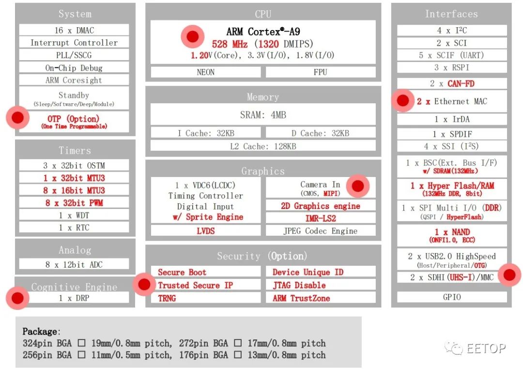
Renesas RZ/A2M Hardware Structure Diagram
The foundation of RZ/A2M is the ARM Cortex-A9 528MHz MPU. Like other MPUs, it has some common peripherals. However, what is special about RZ/A2M is that it is equipped with two network ports, two USB ports, two SDHI, and some security features. In addition, there are three special features that differ from other brands of MPUs; the RZ/A2M is equipped with Renesas’ unique DRP hardware acceleration core, which is mainly used for image preprocessing and is very fast.

It is understood that DRP is a hardware acceleration, which is an external memory-equipped image preprocessing application. It is a self-developed acceleration core by Renesas, which can be about ten times faster than a general CPU. For example, with a 528MHz chip, it can achieve 60 frames output, which is basically equivalent to the FPGA level used by other customers.
So why does RZ/A2M need to use Winbond’s HyperRAM?

In response to this question, Anson, Manager of the Infrastructure Business Unit of Renesas Electronics China introduced that the increasing demand for artificial intelligence in audio/video and other MCU devices is the main reason why companies like Renesas choose HyperRAM products. It is understood that the RZ/A2M is equipped with a 4MB SRAM, which can be used for relatively simple applications, such as some HMI (Human-Machine Interface) or simple control applications. Since it is equipped with the DRP core, even if the CPU does not run fast, it can still be used for image preprocessing. However, facing the current many embedded systems, the data volume and program library are still far greater than ordinary HMI. The 4MB memory capacity is insufficient for many applications in today’s embedded AI systems. Therefore, Renesas often recommends customers to use external memory.
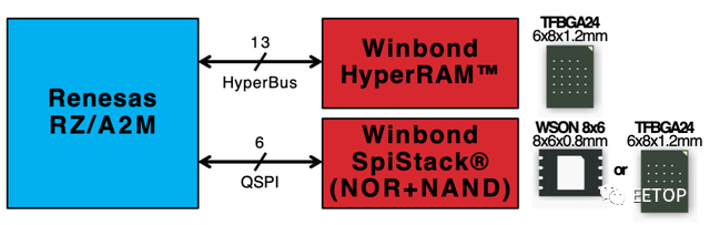
Using Winbond’s HyperRAM and SpiStack (NOR+NAND) allows Renesas RZ/A2M to reduce memory installation area, wire count, and BOM costs on the PCB. Both packaging sizes are only 8x6mm, with 13 signal pins for HyperRAM and 6 for SpiStack (NOR+NAND). Compared to traditional SDRAM and parallel NOR/NAND, Winbond HyperRAM and SpiStack reduce packaging size and terminal count by about 80%. As embedded AI systems become increasingly complex, using the RZ/A2M equipped with external memory can support the increasing data volume of application program code or training models.
— Conclusion —
In the past, traditional storage mainly faced databases, files, and streaming media applications. Today, driven by emerging technologies, storage mainly faces cloud computing, big data, and artificial intelligence in large-scale data application scenarios. In addition, with the trend of miniaturization of IoT terminal devices, a new generation of high-performance, low-power MCU market is emerging. Although the process nodes of MCUs have shifted from 55nm, 40nm to 28nm, and even 16nm, meeting size requirements does not simultaneously lead to optimization of computing power, necessitating a new generation of external memory for data buffering. It is precisely the rise and rapid popularization of these new applications that have brought new opportunities to data storage, and the market demand for storage semiconductor chips is increasing day by day. Of course, opportunities and challenges often go hand in hand. As the industry enters a deep cultivation era, the ability to capture users will determine the future, and finding the right scene for rapid landing will be key.
