
1. Concept of PCBPCB (Printed Circuit Board), known in Chinese as 印制电路板, is an important electronic component that serves as a support for electronic components and provides electrical connections between them. It is called a “printed” circuit board because it is made using electronic printing technology.2. Role and Function of PCB in Various Electronic Devices1. Pads: Provide mechanical support for the fixation and assembly of various electronic components such as integrated circuits. 2. Traces: Achieve wiring and electrical connections (signal transmission) or electrical insulation between various electronic components like integrated circuits. Provide required electrical characteristics, such as characteristic impedance. 3. Green solder mask and silkscreen: Provide solder mask patterns for automatic assembly and identification characters and graphics for component insertion, inspection, and maintenance.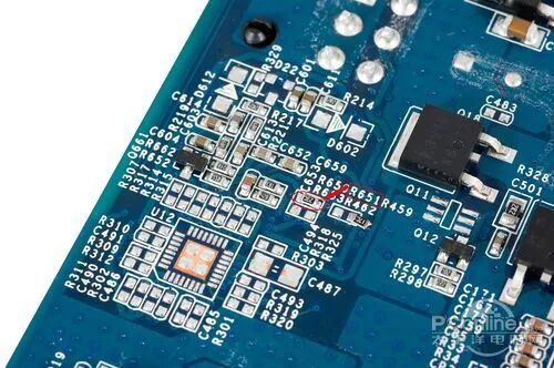 3. Overview of PCB Technology DevelopmentFrom 1903 to the present, the application and development of PCB assembly technology can be divided into three stages:1. Through-Hole Technology (THT) Stage: PCB 1. The role of metallized holes: (1) Electrical interconnection – signal transmission (2) Supporting components – pin size limits the reduction of through-hole size a. Rigidity of pins b. Requirements for automated insertion2. Ways to increase density (1) Reduce the size of component holes, but limited by the rigidity of component pins and insertion accuracy, hole diameter ≥ 0.8mm (2) Reduce trace width/spacing: 0.3mm—0.2mm—0.15mm—0.1mm (3) Increase the number of layers: single-sided—double-sided—4 layers—6 layers—8 layers—10 layers—12 layers—64 layers2. Surface Mount Technology (SMT) Stage: PCB 1. The role of via holes: only serves the purpose of electrical interconnection, and the hole diameter can be as small as possible; blocked holes are acceptable. 2. Main ways to increase density (1) Via hole size drastically reduced: 0.8mm—0.5mm—0.4mm—0.3mm—0.25mm (2) Structural changes in vias: a. Advantages of blind/buried vias: increase wiring density by more than 1/3, reduce PCB size or number of layers, improve reliability, enhance characteristic impedance control, reduce crosstalk, noise, or distortion (due to shorter traces and smaller holes) b. Hole-in-pad eliminates relay holes and connections (3) Thinning: double-sided boards: 1.6mm—1.0mm—0.8mm—0.5mm (4) PCB flatness: a. Concept: The warpage of the PCB substrate and the coplanarity of the connection pads on the PCB surface. b. PCB warpage is a comprehensive result of residual stress caused by thermal and mechanical factors c. Surface coatings of connection pads: HASL, chemical Ni/Au, electroplated Ni/Au…3. Chip Scale Package (CSP) Stage: PCB CSP has begun to undergo rapid transformation and development, driving PCB technology forward, leading the PCB industry into the laser and nano era.

4. PCB Surface Coating TechnologyPCB surface coating technology refers to the solderable coating (plating) layer and protective layer for electrical connections, aside from the solder mask coating (which also provides protection).Classified by purpose: 1. For soldering: The surface of copper must have a coating layer for protection; otherwise, it easily oxidizes in the air. 2. For connectors: Electroplated Ni/Au or chemical Ni/Au (hard gold, containing P and Co) 3. For wire bonding: wire bonding processHot Air Solder Leveling (HASL or HAL) is a method where PCBs coming out of molten Sn/Pb solder are leveled using hot air (230°C).1. Basic requirements: (1) Sn/Pb = 63/37 (weight ratio) (2) Coating thickness at least >3um (3) Avoid the formation of non-solderable Cu3Sn, which occurs due to insufficient tin, such as when the Sn/Pb alloy coating layer is too thin; solder joint composition transitions from solderable Cu6Sn5– Cu4Sn3– Cu3Sn2—non-solderable Cu3Sn2. Process flow: Remove resist—clean board surface—print solder mask and characters—clean—apply flux—hot air leveling—clean3. Disadvantages: a. The surface tension of lead-tin is too high, easily forming a “tortoise shell” phenomenon. b. The surface of the pads is uneven, which is not conducive to SMT soldering.Chemical Ni/Au refers to the process of chemically plating Ni (thickness ≥3um) on the PCB connection pads, followed by plating a thin layer of gold (0.05-0.15um) or a thick layer of gold (0.3-0.5um). Due to the uniformity of the chemical plating layer and good coplanarity, it shows a trend for widespread application. The thin gold plating (0.05-0.1um) is to protect the solderability of Ni, while the thick gold plating (0.3-0.5um) is required for wire bonding processes.1. Role of the Ni layer:a. Acts as a barrier layer between Au and Cu, preventing diffusion between them, which can cause the diffusion area to become loose.b. Serves as a solderable plating layer, with a thickness of at least >3um2. Role of Au: Au serves as a protective layer for Ni, with a thickness between 0.05-0.15; it cannot be too thin, as gold has a high porosity, and if too thin, it cannot adequately protect Ni, leading to Ni oxidation. Its thickness also cannot exceed 0.15um, as gold-copper alloys (Au3Au2) form in solder joints, which can become brittle, and when Au exceeds 3% in solder joints, solderability deteriorates.Electroplated Ni/AuThe structure of the plating layer is basically the same as that of chemical Ni/Au, but due to the electroplating method, the uniformity of the plating layer is somewhat inferior. 5. Precautions for PCB Design Output Production Files1. Layers that need to be output include:(1). Routing layers including top layer/bottom layer/middle routing layers; (2). Silkscreen layers including top silkscreen/bottom silkscreen; (3). Solder mask layers including top solder mask and bottom solder mask; (4). Power layers including VCC layer and GND layer; (5). Additionally, generate drilling files NC Drill.2. If the power layer is set to Split/Mixed, then in the Add Document window, select Routing in the Document item, and before outputting the photoplot files each time, use Pour Manager’s Plane Connect to cover copper on the PCB diagram; if set to CAM Plane, then select Plane and when setting the Layer item, include Layer 25 and select Pads and Vias in Layer 25.3. In the device settings window, change the Aperture value to 199 in Device Setup.4. When setting each layer’s Layer, select Board Outline.5. When setting the silkscreen layer’s Layer, do not select Part Type; select the top layer, bottom layer, and silkscreen layer’s Outline Text Line.6. When setting the solder mask layer’s Layer, select vias to indicate that no solder mask is applied over the vias. Generally, vias will be covered by the solder layer.6. Safety Marking Requirements1. Complete safety markings for fuses: Check if there are six complete markings near the fuse, including fuse number, melting characteristics, rated current value, explosion-proof characteristics, rated voltage value, and English warning markings. For example, F101 F3.15AH, 250Vac, “CAUTION: For Continued Protection Against Risk of Fire, Replace Only With Same Type and Rating of Fuse”. If there is no space on the PCB for English warning markings, they can be included in the product’s user manual.2. High voltage warning symbols in hazardous voltage areas on the PCB: The hazardous voltage area of the PCB should be isolated from the safe voltage area with a 40mil wide dashed line, and high voltage warning symbols and “DANGER! HIGH VOLTAGE” should be printed.3. Clear identification of original and secondary edge isolation zones: The original and secondary edge isolation zones on the PCB should be clearly marked, with dashed lines in between.4. PCB safety markings should be clear and complete.
You Might Need




—— Wei Wenxin, “Printed Circuit World” magazine
Disclaimer: The articles published by this public account are organized or original by Wei Wenxin, and the text and image materials used for customer advertisements are provided by the enterprises. Media reprints of original articles should indicate the source. If there is any infringement, please contact us, and we will delete it as soon as possible. Thank you!