For those working in the electronics industry, it is all about being with PCB all day long, seeing PCB everywhere.PCB is the most fundamental, and precisely because it is fundamental, it is often overlooked. This article will discuss PCB and some commonly used terms in the PCB field.
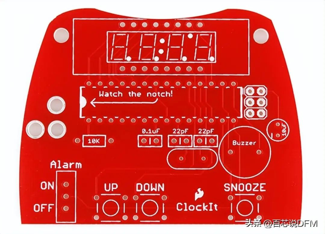
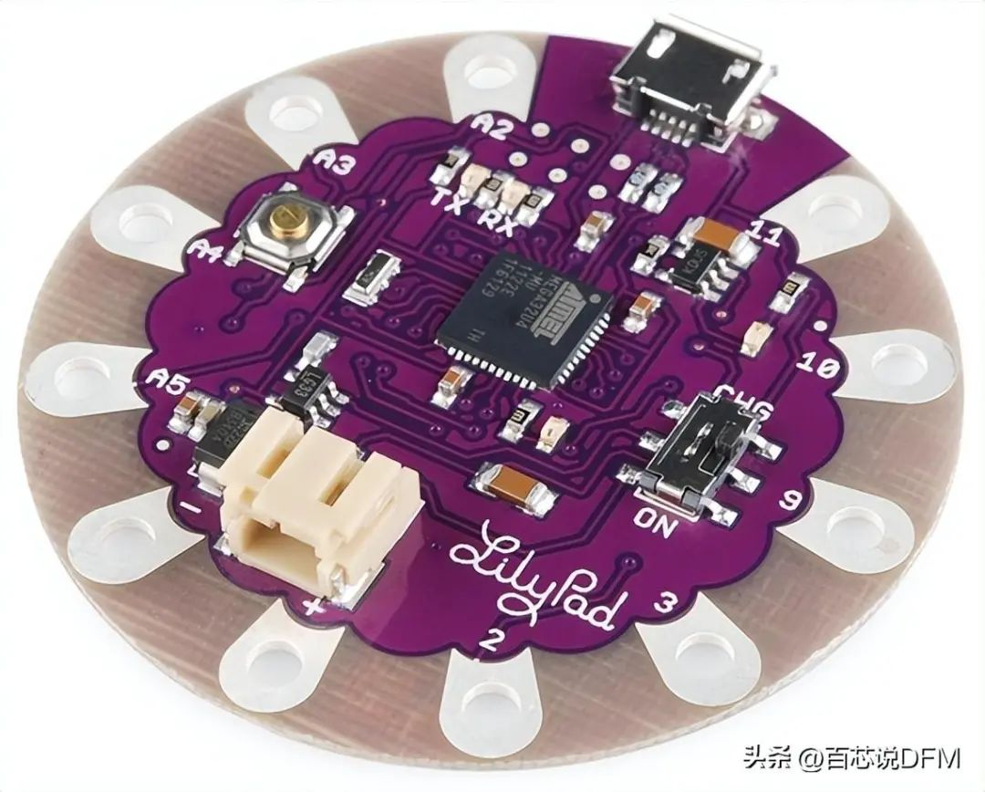
PCB Physical Image
1. What is a Printed Circuit Board?
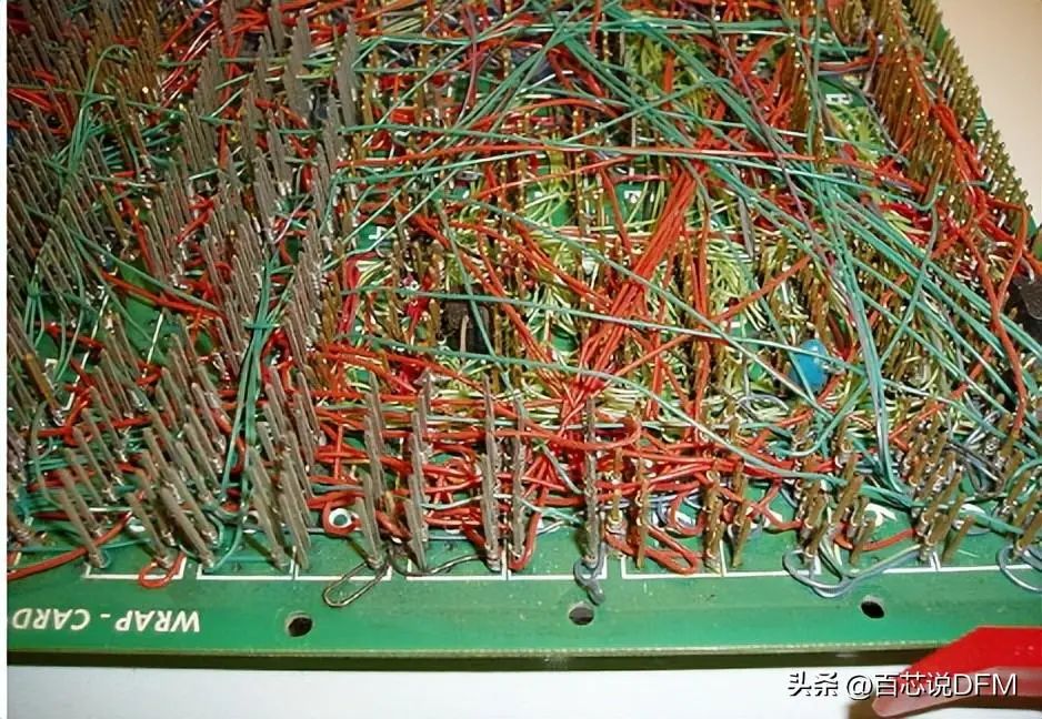
The most common name for a printed circuit board. Before the advent of PCB, circuits were constructed through a laborious point-to-point wiring process. When the insulation layer of the wire begins to age and crack, it often leads to failures and short circuits at the wire connections.
Circuit
As electronic products transitioned from vacuum tubes and relays to silicon and integrated circuits, the size and cost of electronic components began to decrease. Electronic products became increasingly common in consumption, and the pressure to reduce the size and manufacturing costs of electronic products prompted manufacturers to seek better solutions, leading to the birth of PCB.
PCB
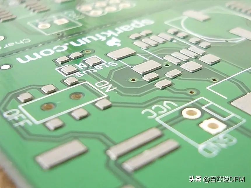
PCB stands for Printed Circuit Board, which is a board with lines and pads that connect various points together. In the above image, there are traces that electrically connect various connectors and components to each other. PCB allows routing of signals and power between physical devices. Solder is the metal used to establish electrical connections between the PCB surface and electronic components. As a metal, solder can also serve as a strong mechanical adhesive.
2. Structure of PCB
PCB is somewhat like a layer cake, as there are alternating layers of different materials, which are laminated together through heating and adhesive, forming a single object.
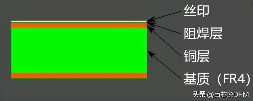
PCB Structure
1. FR4
The substrate is usually glass fiber. Generally speaking, the most common designation for glass fiber is “FR4”. This solid core provides PCB with rigidity and thickness, and there are also flexible PCBs based on flexible high-temperature plastics (Kapton or equivalent materials).
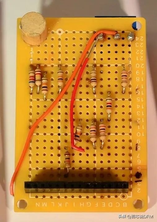
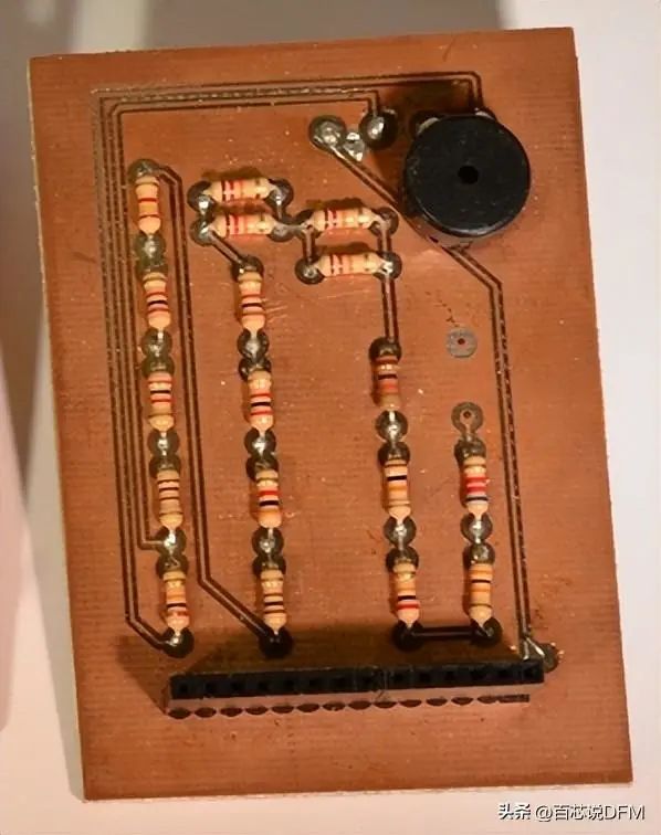
Perforated Board
Cheaper PCBs and perforated boards (as shown above) are made from other materials, such as epoxy resin or phenolic plastic, which lack the durability of FR4 but are much cheaper. When you solder, you often smell a very unique odor, and these types of substrates are commonly used in low-end consumer electronics.
The thermal decomposition temperature of phenolic resin is lower, and when the soldering iron is placed on the circuit board for too long, it can lead to delamination, smoking, and burning.
2. Copper Layer
The next layer is a thin copper foil, laminated to the circuit board through heating and adhesive. In a typical double-sided PCB, copper is applied to both sides of the substrate. In lower-cost electronic products, the PCB may only have copper on one side. When we mention double-sided or 2-layer boards, we refer to the number of copper layers (2) in the baked noodles. This can be as few as 1 layer or as many as 16 layers or more.
PCB Exposed Copper, No Solder Mask or Silkscreen
The thickness of the copper can vary and is specified by weight, in ounces per square foot. The vast majority of PCBs contain 1 ounce of copper per square foot, but some handling very high power PCBs may use 2 or 3 ounces of copper. Each square ounce is approximately 35 microns or 0.0014 inches of copper thickness.
3. Solder Mask Layer
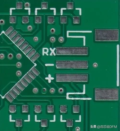
The layer on top of the copper foil is called the solder mask layer. It is usually green (but other colors are also available). The solder mask layer covers the copper layer to prevent copper traces from accidentally contacting other metals, solder, or conductive points. This layer helps users solder in the correct position and prevents solder bridges.
In the example below, the green solder mask layer is applied to most of the PCB, covering fine traces but exposing silver rings and SMD pads for soldering.
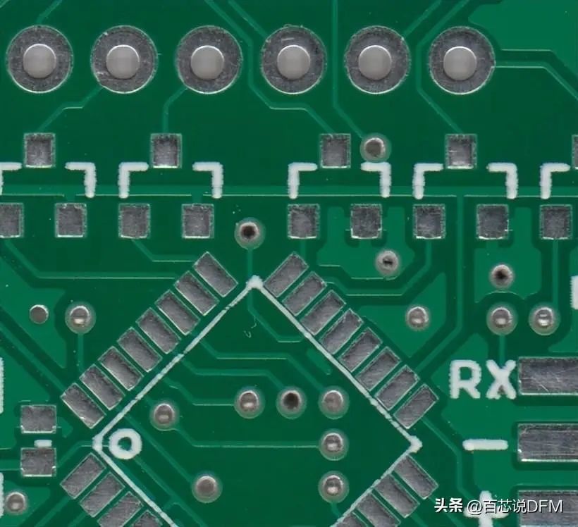
PCB Solder Mask Layer
The most common color for solder mask is green, but there are many other colors. For example: blue, red, white.
4. Silkscreen
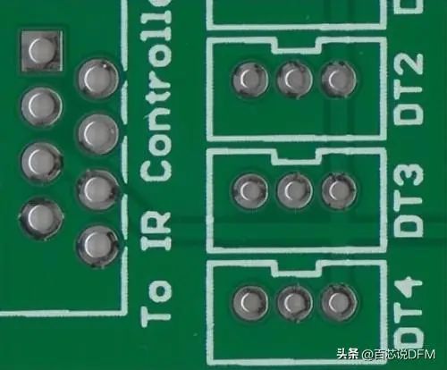
White silkscreen layer is applied on top of the solder mask layer. Silkscreen printing adds letters, numbers, and symbols to the PCB for assembly and indication, allowing people to better understand the circuit board. We often use silkscreen labels to mark the function of each pin or LED.
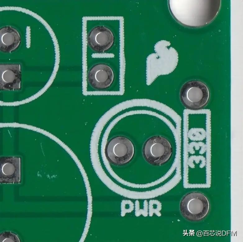
Silkscreen is most commonly white, but any color ink can be used. Black, gray, red, and even yellow silkscreen colors are widely used, but generally, it is quite rare for a PCB to have multiple colors.
3. PCB Terminology
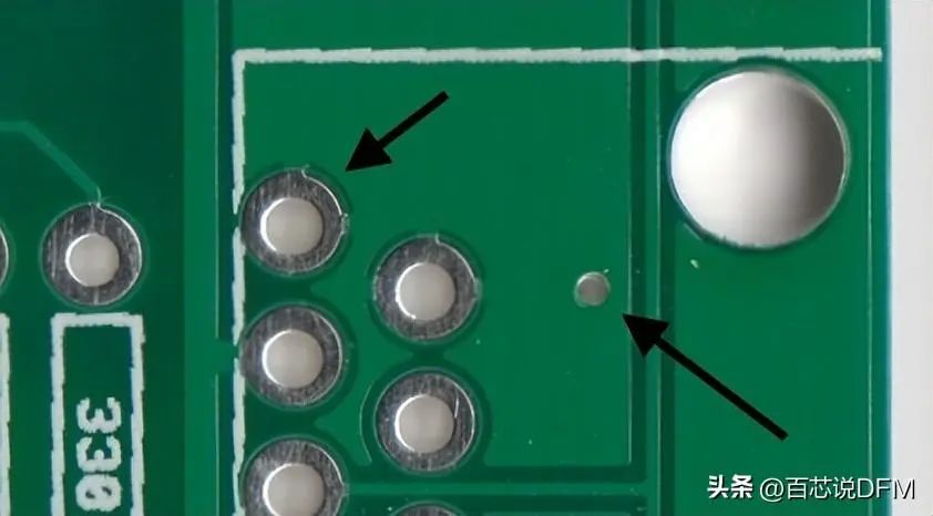
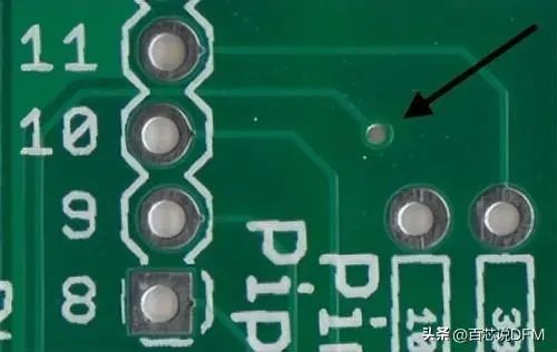
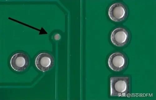
1. Annular Ring
The copper ring around the plated through hole in PCB.
Annular Ring
Annular Ring
2. DRC
Design Rule Check. A software check of the design to ensure that it does not contain errors, such as improper trace contacts, traces that are too thin, or holes that are too small.
3. Drill Hit
The intended position for drilling holes in the design, or where they are actually drilled on the circuit board. Drill hits caused by dull drill bits are a common manufacturing issue.
4. Gold Finger
Metal pads exposed along the edge of the circuit board, used to establish connections between two circuit boards.
Common examples include computer expansion boards or memory boards, as well as the edges of older cartridge-based video games.
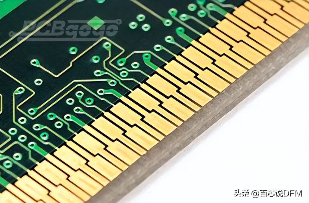
PCB Gold Finger
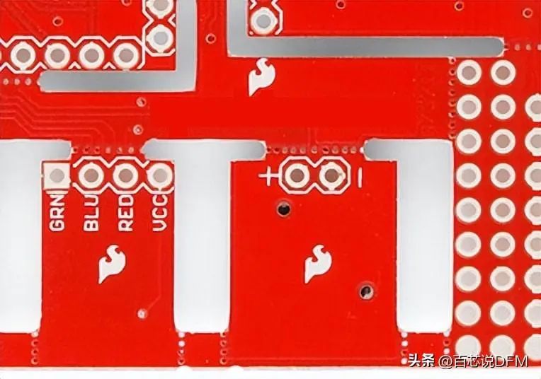
5. Stamped Hole
Stamped holes are used as an alternative method to separate the board from the panel via v-score. Many holes are grouped together to form a weak point, making it easy to break the board afterward.
Stamped Hole
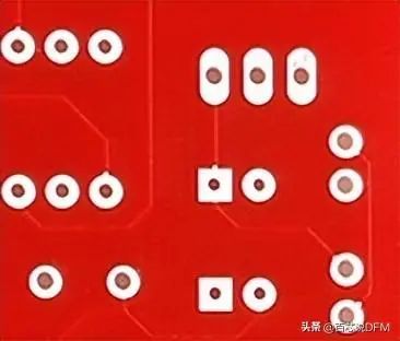
6. Pad
The exposed metal part of the circuit board surface, used for soldering components.
PTH (Plated Through Hole) Pad
SMD (Surface Mount Device) Pad
7. Panel
A larger circuit board composed of many smaller circuit boards, which are separated before use.
Automated circuit board handling equipment often encounters problems when processing smaller circuit boards, and by grouping multiple circuit boards together, processing speed can be significantly increased.
8. Paste Template
A thin metal (sometimes plastic) template on the circuit board, allowing solder paste to be deposited in specific areas during assembly.
9. Pick and Place
The machine or process of placing components on the circuit board.
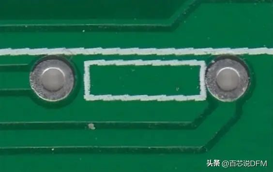
10. Plane
A continuous copper block on the circuit board, defined by boundaries rather than paths, often referred to as “pour”.
Parts of the PCB with no traces, but grounded
1. Plated Through Hole
A hole in the circuit board that has an annular ring and is plated through the circuit board. It may be a connection point for through-hole components, a via for signal passing, or a mounting hole.
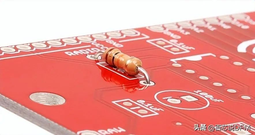
Inserting PTH resistors into the PCB, ready for soldering
Inserting PTH resistors into the PCB, ready for soldering. The legs of the resistors pass through the holes. Plated holes can have traces connecting them on both the front and back of the PCB.
12. Spring Contact
Spring contacts, used for temporary connections for testing or programming purposes.
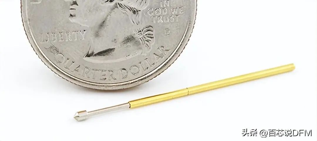
Popular spring contacts with pointed ends
13. Reflow Soldering
Melting solder to form joints between pads and component leads.
14. Silkscreen Printing
Letters, numbers, symbols, and images on the circuit board. Usually only one color is available, and the resolution is generally low.

Silkscreen labeling this LED as a power LED
15. Slot
Any non-circular hole on the board, slots may or may not be plated. Slots sometimes increase the cost of the circuit board because they require additional cutting time.
Complex slots showing many stamped holes
Note: The corners of the slots cannot be made perfectly square, as they are cut with a round end mill.
16. Solder Paste
Small solder balls suspended in a gel medium, applied to the surface mount pads on the PCB before placing components with the help of a solder paste template.
During reflow soldering, the solder in the solder paste melts, forming electrical and mechanical joints between the pads and components.
Solder paste on the PCB just before placing components
17. Soldering Paste
A paste used for quickly hand-soldering circuit boards with through-hole components. Usually contains a small amount of melted solder, quickly dipping the circuit board into it leaves solder points on all exposed pads.
18. Solder Mask Layer
A layer of protective material covering the metal to prevent short circuits, corrosion, and other issues. Usually green, but other colors (SparkFun Red, Arduino Blue, or Apple Black) are also possible. Sometimes referred to as “resist”.
The solder mask layer covers the signal traces but leaves pads to be soldered exposed
19. Solder Bridge
A small amount of solder connecting two adjacent pins on components on the circuit board, according to the design, solder bridges can be used to connect two pads or pins together, which may also lead to unintended short circuits.
20. Surface Mount
A construction method that allows components to be simply mounted on the board without leads passing through holes on the board. This is the primary assembly method used today, allowing for quick and easy assembly of circuit boards.
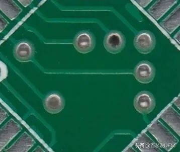
21. Thermal Via
A small trace connecting pads to planes, if pads do not have thermal relief, it can be difficult to get pads to a high enough temperature to form good solder joints. When you try to solder, poorly thermally relieved pads feel “sticky” and reflow takes an unusually long time.
Pads with two small traces (thermal vias) connecting pins to ground. On the right, a via without thermal relief connects it completely to the ground plane
22. Thieving
Shadow lines, grid lines, or copper dots left in areas of the circuit board without planes or traces. Reduces etching difficulty, as it takes less time to remove unwanted copper in the slots.
23. Trace
A continuous path of copper on the circuit board.
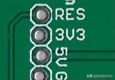
Small traces connecting reset pads to other places on the board. Larger, thicker traces connect to the 5V power pin
24. V-score
A partial cut through the board that allows the board to be easily broken along a line.
25. Via
A hole on the circuit board used to pass signals from one layer to another. Tent vias are covered with solder mask to prevent them from being soldered. Vias that connect connectors and components are usually uncovered (unmasked) for easy soldering.
Front and back of the same PCB showing a tented via
Via
Front and back of the same PCB showing a tented via. This via passes signals from the front of the PCB through the middle of the board to the back.
26. Wave Soldering
A soldering method for circuit boards with through-hole components in which the circuit board is passed through a wave of molten solder, adhering to exposed pads and component leads.
4. How to Design a PCB?
The topic of PCB design is very broad and cannot be explained all at once. Here are some suggestions.
1. Look for CAD software packages
There are many low-cost or free options for PCB design on the market. When choosing, pay attention to the following points:
-
Is therea large user base for the software package? The more users there are, the more likely you are to find ready-made libraries containing the parts you need.
-
Is it easy to use? If it is difficult to use, you won’t want to use it as much.
-
Is it feature-rich? Some may have certain design limitations, such as: number of layers, number of components, circuit board size, etc. Most will allow paid upgrades for features.
-
Convertibility? Some free programs do not allow exporting or converting designs.
2. Learn from others’ layouts
This is the most direct way, learn from others’ layouts, study how others do it. Especially now that there is a lot of open-source material online to learn from, you can learn a lot.
3. Practice, practice, and practice again
4. Lower your expectations
The first circuit board you design will definitely have many issues; even by the time you design your 20th circuit board, there will still be issues. At this time, you need to adjust your mindset; having problems is normal.
5. Schematics
Designing a circuit board without a good schematic usually has one or more problems. So schematics are very important.
That’s all about PCB knowledge, I hope everyone will support it more.
Original link: https://learn.sparkfun.com/tutorials/pcb-basics/all
— END —
Join the Fan Group
(Advertisements and competitors, please refrain)