The A10 processor on the iPhone 7 and iPhone 7 Plus is Apple’s first quad-core design, featuring a big.LITTLE architecture with two high-performance cores and two low-power cores. ChipWorks recently conducted an in-depth disassembly analysis of the various components of the iPhone 7, particularly focusing on the A10 processor, and discovered numerous issues.
The surface number of the A10 processor is APL1W24/339S00255, in contrast to the A9’s APL1022/339S00129 — this is the first time Apple has included letters in the four-digit number of its processors, but it is unclear what this specifically represents.
It can be confirmed that at least the A10 processor in the iPhone 7 A1778 version is manufactured using TSMC’s 16nm FinFET process; theoretically, all processors of this generation should be, but further observation is required.
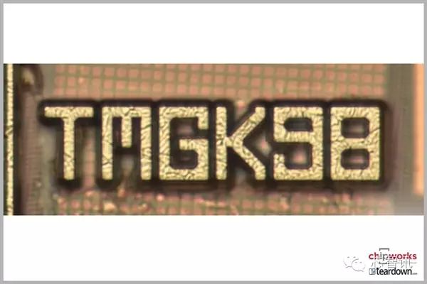
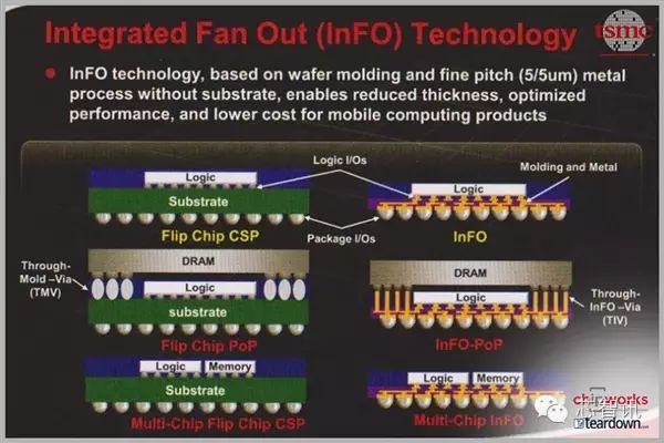
The core number on the processor is TMGK98, continuing from the A9’s TMGK96, with a core area of approximately 125 square millimeters. The packaging uses TSMC’s latest InFO technology, making it more compact than before, with a reported 3.3 billion transistors.
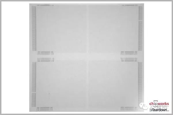
A top view under X-ray shows that the LPDDR4 memory is divided into four blocks rather than stacked together, significantly reducing the chip’s thickness.
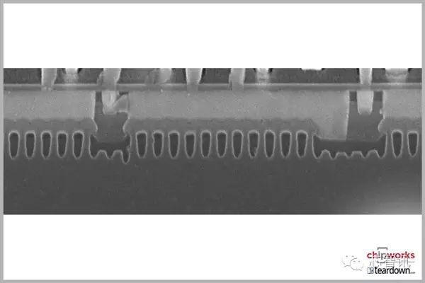
A side view under X-ray.
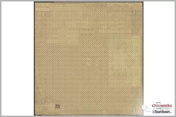
Photo of the metal layer core.
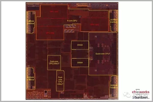
Transistor-level core photo: six GPU cores (divided into three groups), SDRAM memory controller (divided into four groups, likely 128-bit wide), and SRAM cache (divided into two groups) are all clearly visible, with only the positions of the four CPU cores remaining uncertain.
It can be basically confirmed that the two high-performance CPU cores should be located in the middle right position, but it is still uncertain whether the two low-power cores are adjacent to the big cores or in the two areas at the bottom left.
Measurements show that the area of the CPU core region on the right side is approximately 16 square millimeters, which is 3 square millimeters larger than the two cores in the A9; whether this is due to the increase in core size or the addition of small cores remains a mystery.
It is worth mentioning that the authoritative testing software GeekBench can currently only identify the two large cores of the A10.
Editor: Chip News – Linzi
——————————-
Related Articles:
Complete Disassembly of iPhone 7 Plus: Major Internal Design Changes for Waterproofing
The Most Powerful Mobile Processor: Detailed Analysis of Apple’s A10 Chip!
Moore’s Law Failure: What Other Methods Do We Have to Dramatically Increase Computing Performance?
Samsung Negotiates Graphics Chip Technology Licensing with AMD and NVIDIA to Develop Its Own GPU
AMD Unleashes 32 Cores, Intel Responds with 28 Cores!
AMD Plans to Raise $1.02 Billion: New Zen Architecture Targets Intel
The Truth Behind the Samsung Note 7 Recall: Was It Really for Honor?
GlobalFoundries Launches 12nm FD-SOI Process: Performance Comparable to 10nm FinFET at Lower Cost
Detailed Analysis of Intel’s Seventh Generation Core Processor Kaby Lake: 14nm+ Process, Nearly 20% Performance Improvement
Intel Opens Foundry for ARM Chips: TSMC and Samsung Under Pressure
NVIDIA’s Next-Generation Tegra Chip to be Released Next Month: Codename Parker, Upgraded 16nm Pascal GPU
———————————–
For industry communication and cooperation, please add WeChat: xintiyan001
For submissions, please send to: [email protected]
Official Chip News Group: 221807116