Abstract
Introduction
1. CAN Bus and Automotive ECU Bootloader
2. On-chip NVM Resources of S12(X) Series MCU and Driver Development
2.1 Paging Mechanism of S12(X) Series MCU Memory and Introduction to S12G128 On-chip NVM Resources
2.2 Development of S12(X) On-chip NVM Driver
2.3 Detailed Explanation of S19 File
3. Bootloader Design Based on CAN Bus
3.1 PC Host Software and Communication Protocol Design
3.2 Bootloader Host Software Design
3.3 Application Software Design
4. Graphical Rapid Implementation Based on CodeWarrior Processor Expert System
4.1 Introduction to CodeWarrior 5.1 IDE and Processor Expert System
4.2 Memory Allocation for Bootloader and Application Program and Processor Expert System Configuration
5. Conclusion
References
Introduction
Previously, I wrote an article titled “Detailed Points on Automotive Electronic ECU Bootloader Development“, introducing many key points and considerations for the development of automotive electronic ECU BootLoader. The article was entirely theoretical analysis and experience sharing. Many readers have given me feedback, hoping to share some specific practical experiences in automotive electronic ECU BootLoader development.
Based on this, today I would like to share the development of an independent NVM driver bootloader for the S12(X) series MCU based on CAN bus communication, hoping to be helpful and inspiring to everyone. I plan to share the BootLoader development for the MPC57xx series and MagniV S12Z series in the future, so please stay tuned.
1. CAN Bus and Automotive ECU Bootloader
CAN (Control Area Networking) bus– the field control domain network bus is widely used in automotive ECU communication due to its good differential communication anti-interference capability. Currently, the widely adopted CAN bus in automotive ECU is protocol 2.0 A/B, CAN 2.0A only supports 11 bit length ID standard frames, while CAN 2.0B can support extended frames up to 29 bits. The latest CAN bus protocol is CAN FD (Flexible Data rate), which can support a maximum communication rate of 8Mbit/s and a data payload of up to 64 bytes, while being backward compatible with CAN 2.0 A/B protocol [1].
Typical communication rates for CAN 2.0A/B are 125Kbit/s, 250Kbit/s, 500Kbit/s, and the highest 1Mbit/s. In passenger cars, a low-speed CAN network is usually designed with a communication rate of 250Kbit/s and a high-speed CAN network with a communication rate of 500Kbit/s. The low-speed CAN is used for sensor data collection and simple control ECUs, such as automotive window seat adjustment controllers, air conditioning controllers (HAVC), and automotive diagnostics; while the high-speed CAN network is used for interconnecting big data processing and complex control ECUs, such as automotive engine management ECUs, automotive instruments, and electronic power steering ECUs, etc. The interconnection communication between high-speed CAN and low-speed CAN is completed by the body gateway (Gateway) or body control module (BCM).
Bootloader literally means a boot loading program, which is a small program that runs first after the MCU is powered on or reset, permanently residing in the ECU non-volatile memory (NVM Non-Volatile Memory). It initializes the MCU clock, memory, and communication peripherals, monitors whether there are commands to enter the bootloader from the outside, and if so, establishes communication, downloads, parses, and stores the application program into the ECU non-volatile memory area, thus completing the online upgrade function of the application program. Typical common bootloaders include the BIOS system on general PCs. The main functions of the bootloader are:
1. Establish communication with the host PC or remote host to complete the application program download;
2. Parse the format of the application program;
3. Program the parsed application binary code into the ECU non-volatile memory [1].
Once the ECU in automotive electronics is designed and mass-produced, it is difficult to disassemble and return to the parts supplier for functional upgrades or patch repairs. If there are after-sales quality issues, if a recall occurs, both the parts supplier and the vehicle manufacturer will face serious economic losses. Therefore, designing a CAN bus-based ECU online program update bootloader can effectively solve this problem, minimizing the losses for parts suppliers and vehicle manufacturers. Currently, most foreign automotive manufacturers and global Tier 1 automotive parts suppliers require the implementation of bootloader functionality in their designed ECUs.
2. On-chip NVM Resources of S12(X) Series MCU and Driver Development
The S12(X) series MCU is a 16-bit automotive-grade MCU developed by NXP specifically for automotive body control and engine control ECU applications, currently widely adopted by major parts suppliers, with annual shipments exceeding one billion units. Here, we mainly introduce the on-chip NVM (Non-Volatile Memory, including on-chip EEPROM and Flash) resources of the S12G series for general body control applications and the S12XE series for engine control applications.
The memory addressing capability of an MCU (i.e., its addressing range size) depends on its system address bus, closely related to the core used by the MCU. Generally, the width of the stack register in the CPU and the program counter register is the same as the address bus. In the S08 and S12(X) cores, both the SP and PC registers are 16-bit wide, so their maximum linear addressing range (or direct addressing range) is 216=64KB.
However, automotive electronic applications are becoming increasingly complex, and user application programs need to continue to increase. The 64KB storage space can no longer meet the demand. Some automotive MCUs with more than 64KB Flash have emerged, such as 128KB P-Flash S08DZ128, 128KB P-Flash S12G128, and 1MB P-Flash S12XEP100 MCUs. To efficiently access P-Flash storage space larger than 64KB, Freescale proposed a memory paging access mechanism. That is, access to the paged Flash space is performed through a 16KB Flash window from 0x8000~0xBFFF in a memory-mapped manner [2].
Therefore, before introducing the development of the S12(X) NVM driver, it is necessary to first introduce the memory paging working mechanism of the S12(X) series MCU.
2.1 Paging Mechanism of S12(X) Series MCU Memory and Introduction to S12G128 On-chip NVM Resources
First, let’s introduce some commonly used address definitions during memory paging access of the S12(X) series MCU:
Local Address: Also known as the local address, refers to the address that the CPU can directly access linearly. For a 16-bit MCU, it is the 0x0000~0xFFFF 64KB address space. The local address space is also called the non-paged area (NON_BANKED), and the CPU can efficiently address it. The interrupt service functions of the application program and the startup information of the application project must be placed in the non-paged area;
Logical Address: Also known as the virtual address, is the address used in the link file .prm and memory mapping file .map as well as the default CodeWarrior compilation results and the addresses used in the S19 file. Its address space is a discontinuous space in units of 16KB, generally in the form of P-Flash page number (Flash page number) stored in the memory mapping controller PPGAE register (address 0x0015 in S12G), used to index the logical address when accessing Flash through the paging window) + Flash paging window address (0x8000~0xBFFF). For example, the logical address corresponding to Page C of Flash is: 0xC8000~0xCBFFF, while the logical address corresponding to Page E of Flash is 0xE8000~0xEBFFF;
Global Address: Also known as the physical address, is the linear continuous address space assigned to P-Flash by the chip during design. It is used when operating on P-Flash (e.g., writing P-Flash driver programs, erasing, writing, etc.) and is also the address used in the .phy file. For S12/S12X series MCUs, the .phy file can be converted from the S19 file using P&E Log2Phy software.
The mapping relationship between the local address and global address of the S12G series MCU is shown below:
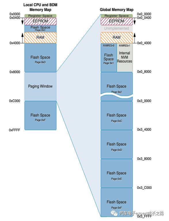
Figure 1. Mapping Relationship Between Local Address and Global Address
Here, taking the typical S12G128 as an example, its P-Flash resource address mapping is as follows:
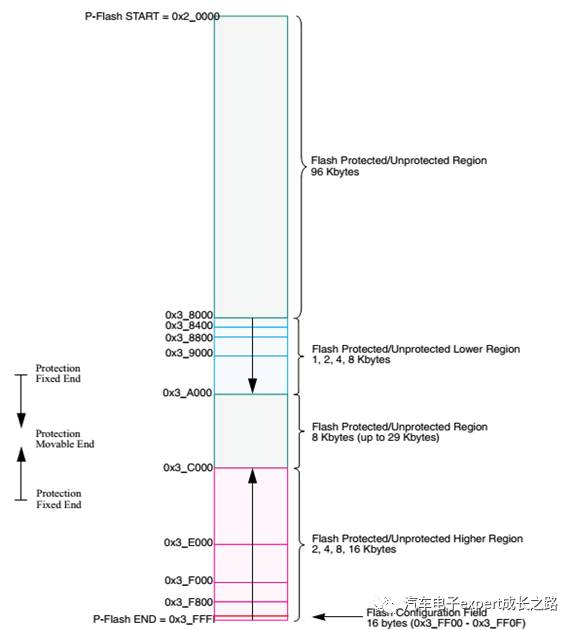
Figure 2. S12G128 On-chip NVM Resource Mapping
The 128KB Flash of S12G128 includes 8 consecutive 16KB Flash pages starting from the global address 0x20000, which supports region protection of 1/2/4/8/16KB and the encryption of the entire P-Flash. The so-called protection means that it cannot be erased and rewritten by the application program. This function is often used in bootloader development to protect the bootloader program itself from being modified by the application program, as the bootloader is the foundational program for online upgrades of the ECU, needing to reside in the ECU for a long time. The encryption is for the BDM debugging interface, but after encryption, the only command that an external debugger can execute on S12G is mass erase, and to decrypt, one must execute the mass erase command to clear all data on the P-Flash or use an 8-byte backdoor key (located at local address 0xFF00~0xFF07, global address 0x3FF00~0x3FF07) for decryption, thus preventing normal access (reading or writing) to the on-chip P-Flash resources through the BDM interface, effectively protecting the user’s software intellectual property.
Tips: Different parts of the S12(X) series MCUs have different mapping relationships between local, logical, and global addresses, and the logical address numbers may also vary. Additionally, their RAM, EEPROM, and other memories may also have paging situations (e.g., S12XE and S12XHZ/Y series MCUs). Please refer to their respective datasheets/reference manuals for specifics.
2.2 Development of S12(X) On-chip NVM Driver
Operations on the on-chip Flash and EEPROM of the S12(X) series MCU are completed through the general command target registers for Flash operations FCCOBIX/FCCOB, writing operation addresses, data, and commands, and combining with the status register FSTAT to form command sequences. A typical NVM command write sequence flowchart is shown below:
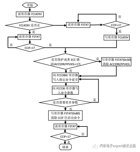
Figure 3. Flash Command Write Sequence Flowchart
Typical S12(X) NVM operations include erasing, programming, verification, etc. The complete NVM commands and their modes and encryption state permissions are shown in Table 1:
Table 1. NVM Commands and Their Modes and Encryption State Permissions
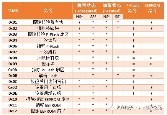
(1 Decrypt normal single-chip mode; 2 Decrypt special single-chip mode; 3 Encrypt normal single-chip mode; 4 Encrypt special single-chip mode)
The user can use the Processor Expert system in CodeWarrior 5.1 IDE to graphically configure and generate these NVM operation driver API functions, or directly use the standard driver code (SSD) provided by NXP on their official website. The latter provides runtime-independent source code, S19 files, C arrays, and static libraries in various forms for more flexible use [4].
Since the NVM driver in this design needs to be separated from the bootloader and downloaded to RAM from the host PC via the CAN bus for execution, the official standard driver (SSD) is used in C array form, compiled into a 4KB RAM space starting at 0x3000 and generating a function address table, forming an S19 file, which is then merged with the application program’s S19 file (to ensure the normal operation of the NVM driver, it must be ensured that the merged S19 file has the NVM driver at the front), and downloaded together. In the bootloader, function pointers are used for function calls.
The method for creating an independent NVM driver is as follows: First, configure the SSD according to the actual MCU model (located in the SSD installation directory\drvsrc\include\SSD_SGF18.h in the FLASH_DERIVATIVE definition), make (double-click to run the SSD installation directory\drvsrc\make\make.bat command batch file) to generate the C array form of the NVM driver (located in the SSD installation directory\driver\c-array_driver directory), organize it into a C file along with the SSD header files (the three header files in the SSD installation directory\drvsrc\include directory) added to the CodeWarrior 5.1 project, and place the addresses of each NVM driver function in an array located at address 0x3F80 (using the CodeWarrior address specifier “@” to specify the data storage address) as the NVM driver function address table. Since all NVM driver function arrays and the NVM driver function address table are modified by the C language keyword const, they are array constants, which are by default placed in the ROM_VAR segment. Modifying the project PRM link file to place the ROM_VAR segment in the allocated NVM_RAM can compile the NVM driver to the RAM address starting at 0x3000, obtaining the S19 file, and separating the S19 format file of the NVM driver and its function address table from the S19 file.
The specific NVM driver function mapping address table and project link file are shown in the figure below:
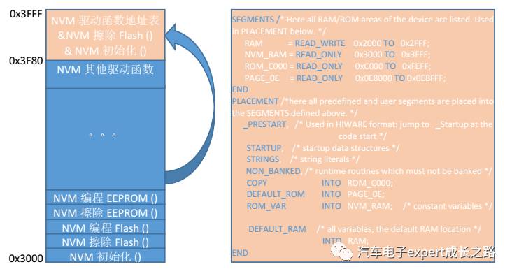
Figure 4. NVM Driver Function Mapping Address Table and Project Link File
Tips: NVM independent drivers are flexible and customizable. For basic bootloader functions, it is sufficient to initialize init(), erase EEPROM/P-Flash erase(), program EEPROM/P-Flash program(), and verify EEPROM/P-Flash verify() functions. Therefore, necessary NVM driver functions can be selected according to the bootloader’s functionality, thus reducing the RAM space occupied to accommodate small RAM-sized MCUs (e.g., S12GN16/32 series with 1KB RAM), of course, the compilation address and NVM driver function mapping address table also need to be changed.
Table 2. Comparison of On-chip Memory and Peripheral Resources of S12G Series MCU
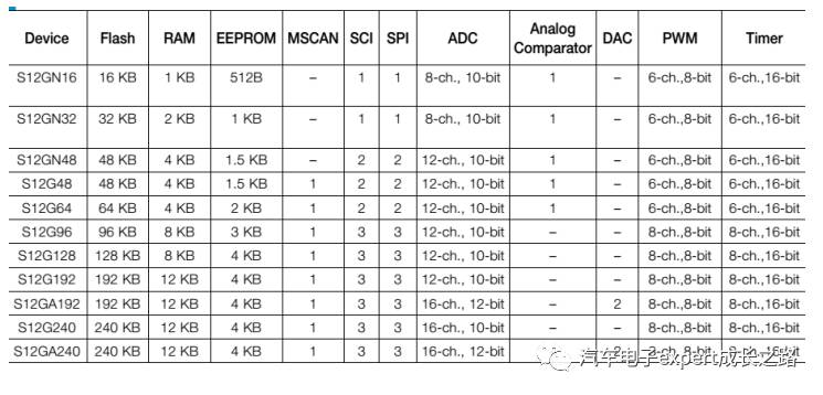
Tips: For the memory paging access mechanism of the S12(X) series, please refer to the articles in this public account:
a. “Detailed Explanation of On-chip Memory Resources and Paging Access Mechanism of S12(X) Series MCU (Part 1)“;
b. “Detailed Explanation of On-chip Memory Resources and Paging Access Mechanism of S12(X) Series MCU (Part 2)“;
2.3 Detailed Explanation of S19 File
The host PC or bootloader must parse the compiled result file of the application program to obtain programming addresses and information, so it is essential to understand the format of the compiled result file when developing the bootloader. The S12(X) series MCU’s CodeWarrior 5.1 IDE compilation result is an S19 file, so the following will provide a detailed introduction.
The S19 file, also known as the S-record file, is the default compilation result file of the CodeWarrior 5.1 IDE, developed and led by Motorola, and is one of the three commonly used programming file formats for embedded MCU EEPROM/Flash, along with Intel’s HEX file and bin file.
The content of the S19 file is ASCII encoded and can be opened and viewed with any text editor. Each line of its content starts with the ASCII code letter “S” and uses 0-9 as identifiers for different types of lines, where “S0” is the S19 file information, which is meaningless for programming, while “S1~S9” indicates the information that is truly related to programming, hence the name. The specific format and definition of each line in the S19 file are as follows:

Figure 5. S19 Line File Format
Type (Type) : 2 characters. Used to describe the type of record (S0, S1, S2, S3, S5, S7, S8, S9).
Count (Count) : 2 characters. Used to form and indicate a hexadecimal value, showing the count of remaining pairs of characters in the record.
Address (Address) : 4 or 6 or 8 bytes. Used to form and indicate a hexadecimal value, showing the address where the data should be loaded. The length of this part depends on the number of bytes in the load address. A 2-byte address occupies 4 characters, a 3-byte address occupies 6 characters, and a 4-byte address occupies 8 characters.
Data (Data) : 0—64 characters. Used to form and indicate a hexadecimal value representing the memory load data or description information.
Checksum (Checksum) : 2 characters. When these characters are paired and calculated into hexadecimal data, they form a least significant character byte, which is used to express the complement of the data, address, and database character pairs represented by the (byte) complement sum. That is, the count value, address field, and data field’s several characters are paired into two characters, summed, and the overflow part is not counted, only the lowest two characters are retained NN, checksum =0xFF-0xNN.
S0 Record: The record type is “S0” (0x5330). The address field is not used, set to zero (0x0000). The information in the data field is divided into the following four subdomains:
-
Name (Name) : 20 characters, used to encode the unit name
-
Version (Version) : 2 characters, used to encode the version number
-
Reversion (Revision) : 2 characters, used to encode the revision version number
-
Description (Description) : 0-36 characters, used to encode text comments
This line indicates the start of the program and does not need to be burned into memory.
S1 Record: The record type is “S1” (0x5331). The address field is indicated by a 2-byte address. The data field consists of loadable data.
S2 Record: The record type is “S2” (0x5332). The address field is indicated by a 3-byte address. The data field consists of loadable data.
S3 Record: The record type is “S3” (0x5333). The address field is indicated by a 4-byte address. The data field consists of loadable data.
S5 Record: The record type is “S5” (0x5335). The address field is indicated by a 2-byte value, containing the count of previously transmitted S1, S2, S3 records. There is no data field.
S7 Record: The record type is “S7” (0x5337). The address field is indicated by a 4-byte address, containing the start execution address. There is no data field. This line indicates the end of the program and does not need to be burned into memory.
S8 Record: The record type is “S8” (0x5338). The address field is indicated by a 3-byte address, containing the start execution address. There is no data field. This line indicates the end of the program and does not need to be burned into memory.
S9 Record: The record type is “S9” (0x5339). The address field is indicated by a 2-byte address, containing the start execution address. There is no data field. This line indicates the end of the program and does not need to be burned into memory.
Tips:
A. In the same S19 file, there may be S2/3/4 three different data record lines simultaneously;
B. Depending on different description information, choose one of the above S7/8/9 different end lines to use.
3. Bootloader Design Based on CAN Bus
The design of the bootloader based on the CAN bus includes two parts: the host software running on the PC and the bootloader host software running on the target MCU.
3.1 PC Host Software and Communication Protocol Design
The main function of the host software running on the PC is to read the application program S19 file of the target MCU and call the USB to CAN bus adapter (Adapter) to download it line by line to the target MCU, and the software design flowchart is as follows:
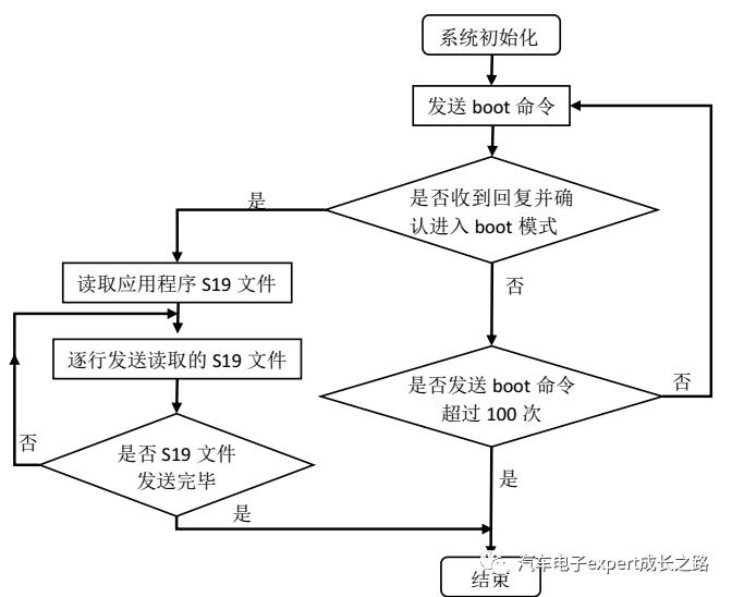
Figure 6. PC Host Software Design Flowchart
In this design, Visual C++ is used to call WFC and the Wuhan Jiyang Optoelectronics -GY8507 USB to CAN adapter driver to write the host interface software.
The CAN message for downloading the application program S19 file from the PC host is a standard data frame with ID 0x64, while the bootloader host program responds to the CAN message frame from the host PC with a standard data frame with ID 0xC8, and the communication rate is set to 500Kbit/s. Therefore, during S12G initialization, the MSCAN module’s receive ID filter is set to only receive standard frames with ID 0x64 to avoid interference from other ECUs on the normal network. In actual implementation on the vehicle, the communication rate is determined by the current CAN network where the ECU is located, and the message ID for communication is defined by the vehicle manufacturer. The specific CAN message command definitions are as follows:
Table 3. Bootloader Communication CAN Message Command Definitions
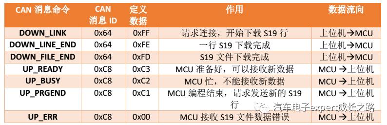
3.2 Bootloader Host Software Design
The design flow of the bootloader host software is shown in the figure below:
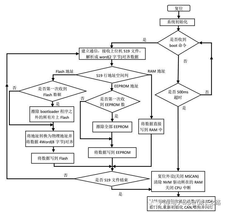
Figure 7. Bootloader Host Software Design Flowchart
After each reset of the MCU (including power-on reset, watchdog reset, external input reset, low voltage detection reset, clock detection reset, and illegal address reset), system initialization is performed, configuring the system clock, turning on the timer, configuring MSCAN and GPIO for status indication, enabling CPU global interrupts, and then waiting for the host PC boot command and checking for timeout: if a request to enter boot is received from the host PC within the specified 500ms, data is received and parsed to obtain line addresses and word-aligned data (1 word = 2 Bytes), then judging the S19 line address space. If it is a Flash address and the first Flash data is received, all on-chip Flash except the bootloader program will be erased to prepare for programming the application program; if it is an EEPROM address and the first EEPROM data is received, all EEPROM will be erased; if it is a RAM address, nothing will be erased. For Flash address data, before programming into Flash, the local/logical addresses in the parsed results must be converted to the linear continuous physical addresses required by the Flash driver, and the data must be 4-word aligned to improve programming efficiency. Then, communication with the host PC is established, receiving line by line, parsing, and writing the results to the corresponding addresses in the on-chip Flash/EEPROM/RAM until the entire application program S19 file ends. Finally, peripherals are reset (turning off MSCAN), clearing the RAM space where the NVM driver is located, turning off CPU global interrupts, disabling all peripheral interrupts, and ending the bootloader to jump to the application reset function to start executing the application program; if the boot command from the host PC via CAN is not received within the specified 500ms, the CPU global interrupts are directly turned off, all external interrupts are disabled, and the bootloader ends to jump to the application reset function to start executing the application program.
3.3 Application Software Design
In application program design, it is necessary to set IVOR=0xEF during system initialization to offset the application program interrupt vector table to 0xEF80, separating it from the default interrupt vector table of the MCU after reset at 0xFF80, thus executing different peripheral interrupt service functions.
Additionally, the COP watchdog needs to be enabled, and in the main loop of the application program, the watchdog should be fed normally, while in the MSCAN receive interrupt, the received CAN message ID should be checked. If the Boot ID is received, it enters an infinite loop, causing the watchdog to overflow and reset the MCU, thus entering the bootloader.
Therefore, a typical application program software design flowchart is shown below:
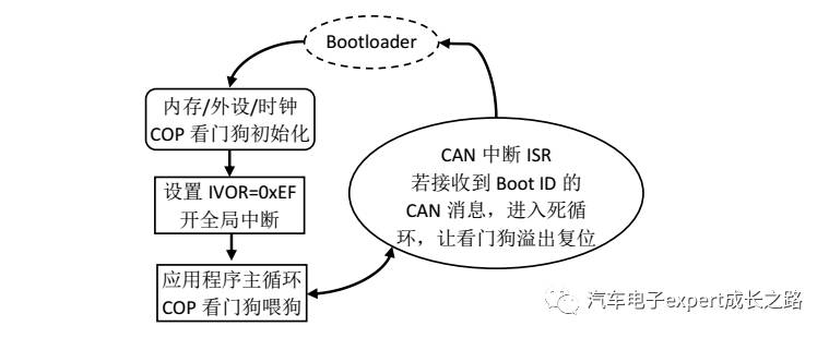
Figure 8. Typical Application Program Software Design Flowchart
4. Graphical Rapid Implementation Based on CodeWarrior Processor Expert System
4.1 Introduction to CodeWarrior 5.1 IDE and Processor Expert System
CodeWarrior 5.1 IDE (Integrated Development Environment) is an integrated development environment developed by NXP that supports the entire S12(X) series MCU, integrating all major tools necessary for building and application – IDE, compiler, debugger, editor, linker, assembler, etc. It integrates advanced debugging technology with a robust development environment, bringing C/C++ source-level debugging and embedded application development to a new level. The IDE provides a highly visual and automated framework that can accelerate the development of even the most complex applications, making it easy and convenient for developers of all levels to create applications. This article introduces the use of CodeWarrior 5.1 IDE as the software development tool.
The integrated Processor Expert system of CodeWarrior 5.1 IDE is a mass production-level automatic code generation graphical configuration tool specifically for the S12(X) series MCU core and peripheral driver development.
When using it, simply enable the use of Processor Expert selection in the project creation wizard (default is None, not used) to create a Processor Expert project. Each peripheral of the MCU is called a component, and users can add corresponding components from the component library according to their needs to graphically configure the corresponding peripherals. Configuration of CPU interrupts, system clocks, and memory allocation is completed in the default CPU component added during project creation. During the configuration process, the Processor Expert system automatically checks for conflicts between the configurations of various peripheral resources, and code can only be generated normally when all peripheral configurations are correct.
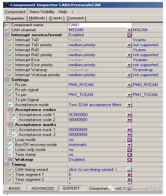
Figure 9. Processor Expert System Peripheral Component (FreescaleCAN)
In the CPU component, there will be additional compilation options and usage options, where the compilation options are used to configure the MCU’s memory and link files (prm), and the configuration of the project stack size is of concern; the usage options are used to configure whether the on-chip resources are used for Processor Expert system configuration and to statistically indicate which specific components are used.
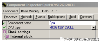
Figure 10. Processor Expert System CPU Component
Each time the project is compiled, the Processor Expert system automatically updates and synchronizes the configuration of the CPU and peripherals, maintaining the automatically generated code. Each component will generate a .c and .h file named after the component, located in the “Generated Code” folder (the code in this folder cannot be modified by the user and will be automatically overwritten each time code is generated). User-programmable code is placed in the “User Module” folder, where the main function is located in the .C file named after the project, and event.h and event.c are for interrupt callback functions (call back function), where users write interrupt service functions. Users only need to add their interrupt handling code in the corresponding interrupt callback function to complete interrupt handling without worrying about clearing interrupt flags, as the interrupt ISR generated by the Processor Expert system has already cleared the corresponding interrupt flags.
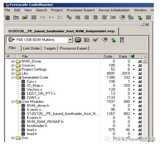
Figure 11. Project Directory After Automatic Code Generation by Processor Expert System
Tips: Each Processor Expert component has detailed help documentation explaining its configuration and usage, which will not be elaborated here.
4.2 Bootloader and Application Program Memory Allocation and Processor Expert System Configuration
In the bootloader project, the Processor Expert system is used to configure an external 8MHz crystal oscillator as the PLL reference clock, configure the PLL frequency output 50MHz as the CPU running clock, and the divided 25MHz as the bus clock frequency; MSCAN communication rate is 500Kbit/s, enabling receive interrupts. Configure the space from 0xF000 to 0xFEFF as the bootloader storage space of 3.8KB, stack size of 256B, and reserve the space from 0x3000 to 0x3FFF as the storage and running space for the NVM driver code and initialize it to 0. Change the default ROM_C000 page address to 0xC00E to 0xEFFF, and the system RAM space is from 0x2000 to 0x2FFF.
In the application program project, it is necessary to reserve the last 4KB space of Flash where the bootloader is located, and the remaining Flash space can be fully used by the application program; for RAM space, all 8KB can be used by the user. However, it must be ensured that the entry function Entry_Point() is located at address 0xC00E (because in the project generated by the Processor Expert system configuration, the default interrupt service functions Cpu_Interrupt() and the assembly software delay function Cpu_Delay100US() occupy 2 bytes and 12 bytes respectively, and then the MCU reset interrupt service function _EntryPoint() is placed, if the assembly software delay function Cpu_Delay100US() is not enabled in the CPU component of the Processor Expert system, then the entry address of the bootloader and application program should be changed from 0xC00E to 0xC002).
Tips: If the application program’s reset vector (in this example, 0xEFFE) is used to extract the reset function address of the application program, and then the function pointer assignment jump method is used to jump to the application program, there is no need to consider the reset function address change caused by the increase of the program in the application program.
#define APP_StartAddr (*(uint16_t*)0xEFFE)/*get the reset function address from app reset vector*/
typedef void (* Jump_Func)(void); /*define a void function pointer*/
(*(Jump_Func)(APP_StartAddr))(); /*jump to app _start*/
or:
(*(void (*)(void))(APP_StartAddr))();/*jump to app _start*/
The memory allocation of the Bootloader and application program introduced in this article is as follows:
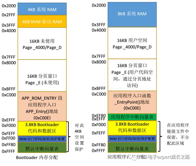
Figure 12. Bootloader and Application Program Memory Allocation
Using the compilation options of the Processor Expert system CPU component can conveniently and quickly complete the above memory allocation and generate the prm link file. The bootloader memory allocation Processor Expert system configuration results are as follows:
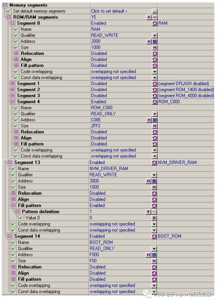
Figure 13. Bootloader Memory Allocation Processor Expert System Configuration
The corresponding link file automatically generated by the Processor Expert system is as follows (the blue highlighted parts are the PRM link file keywords or system reserved segments):
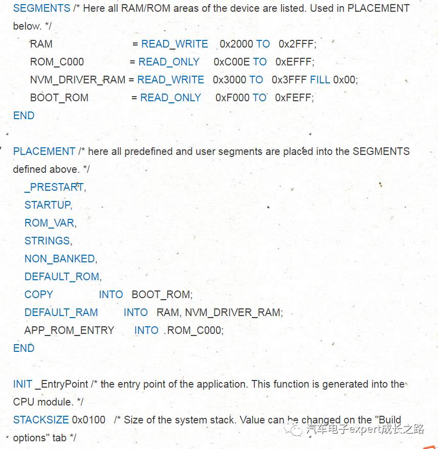
Tips: For detailed usage of the prm file in CodeWarrior IDE, please refer to the article in this public account “Detailed Explanation of prm Link File Usage in CodeWarrior IDE (Custom Memory Partitioning and Custom RAM Data Initialization and Running Functions in RAM)”;
5. Conclusion
This article addresses the practical needs of bootloader development for the S12(X) series automotive-grade MCU from NXP in automotive ECU applications, introducing the on-chip non-volatile memory (NVM) resources of the S12(X) series MCU and driver development, proposing and implementing a safe bootloader design based on CAN bus that downloads the NVM driver program from the host PC to run in RAM instead of residing in the MCU on-chip Flash, effectively avoiding program/data loss caused by the application program running off the on-chip Flash NVM driver code. With the help of the graphical peripheral configuration and automatic code generation tool in CodeWarrior 5.1 IDE – Processor Expert System, the memory allocation and on-chip peripheral configuration of the bootloader and application program are conveniently realized. This design provides a reference for practical engineering applications, allowing customers to modify the CAN message boot ID and commands based on the requirements of the vehicle manufacturer and add corresponding UDS or CCP protocol stacks to quickly develop a safe bootloader product that meets the manufacturer’s requirements.
Tips: The BootLoader development host and app project, NVM SSD driver installation package for S12G series MCU, host GUI software, and detailed user manual mentioned in this article have been packaged and shared in the following Baidu Cloud link for your reference and study:
Link: http://pan.baidu.com/s/1i5N7EbN
Password: p5n6
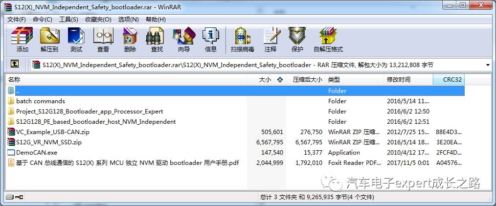
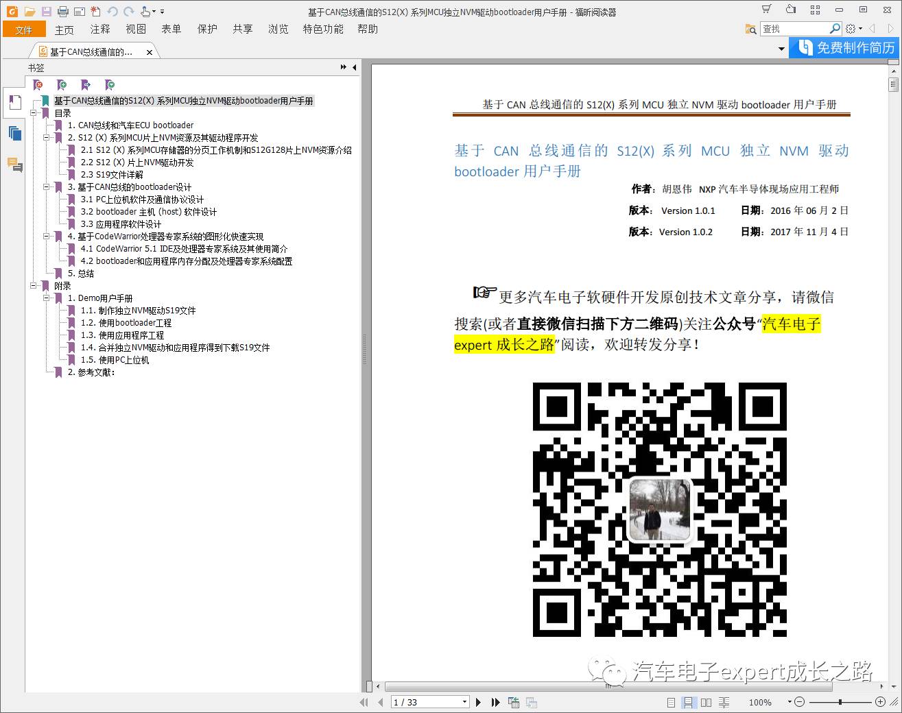
The following image is a screenshot of the BootLoader user manual mentioned in this article:
References
[1]. [Konrad Reif, ed., translated by Sun Zechang et al., BOSCH Automotive Electrical and Electronics, Chinese Second Edition. 2014.8.
[2]. AN3784. Understanding the Memory Scheme in the S12(X) Architecture, Application Note. NXP Semiconductor, http://www.nxp.com. 2009.
[3]. MC9S12G Family Reference Manual, Rev.1.25. NXP Semiconductor, http://www.nxp.com. 2014.
[4]. Standard Software Driver for MC9S12G / MC9S12VR User’s Manual, Rev.3.1. NXP Semiconductor, http://www.nxp.com. 2012.
That concludes the content I wanted to share with everyone today. I hope it is useful to you.
Original writing is not easy. If you find this article helpful for your work and study, you are also welcome to reward and encourage me —- I will continue to write and bring you more exciting original articles.
Tips: Readers using Android phones can directly click the reward link at the end of the article; readers using iPhones can scan the QR code below to reward and encourage the author, as Apple has closed the WeChat reward function.
Thank you!






This public account has published personal original high-quality embedded system technology articles, and the links are as follows. You are welcome to refer to and share:
-
Series of Articles on the Growth Path of Automotive Electronics Expert Public Account
-
Detailed Points on Automotive Electronic ECU Bootloader Development
-
Discussion on Three Common Misunderstandings in Embedded MCU Development
-
Discussion on Heap and Stack in Embedded MCU Software Development
-
Discussion on Interrupt Priority and Interrupt Nesting in Embedded MCU Software Development
-
Discussion on Code Style and Code Optimization in Embedded MCU Software Development
-
Discussion on the Startup Process in Embedded MCU Software Development (Preparation Work from Reset Vector to Main Function)
-
Discussion on the Startup Process in Embedded MCU Software Development (Implementing Custom Initialization in RAM in CodeWarrior 5.1)
-
Discussion on Three Writing Methods of Interrupt ISR in S12(X) Series MCU in CodeWarrior 5.1 IDE
-
Discussion on Minimum System Circuit Design of MCU in Embedded MCU Hardware Design
-
Detailed Explanation of On-chip Memory Resources and Paging Access Mechanism of S12(X) Series MCU (Part 1)
-
Detailed Explanation of On-chip Memory Resources and Paging Access Mechanism of S12(X) Series MCU (Part 2)
-
Principles of Encryption (Secure) and Decryption (Unsecure) of S12(X) Series MCU
-
Using Cyclone Offline Programmer to Program On-chip NVM of S12(X) and MagniV S12Z Series MCU
-
Full Analysis of the Startup Process of Qorivva MPC56xx Series MCU (Based on CW IDE Application Project — EAB I, Link File, Startup File, and Map File)
-
CodeWarrior IDE Usage Tips – Full Analysis of Map File for Qorivva MPC56xx Application Project (CW 2.10/10.x)
-
Mode Control and Switching of Qorivva MPC56xx/57xx Series MCU (On-chip Peripheral Resource Enablement and Power Control)
-
S32K1xx Series MCU Usage Tips — Function Introduction and Software Development and Hardware Design FAQ
-
S32K1xx Series MCU Usage Tips — Solving the Problem of Inability to Connect to Debugger After Flash Encryption
-
Peripheral Usage Tips for MSCAN Receive ID Filter Settings
-
Peripheral Usage Tips for TIM Timer Usage FAQ and Experience
-
Peripheral Usage Tips for SWT Watchdog Timer Configuration and Usage of MPC574xP Series Automotive MCU
-
S32DS Usage Tips — Migration and Upgrade Methods and Precautions from S32DS for ARM v1.3 to S32DS for ARM V2.0
-
S32DS Usage Tips — Project Property Configuration (Compilation Options and C Compiler, Assembler, and Linker Settings)
-
S32DS Usage Tips — How to Compile and Call Static Libraries
-
S32DS Usage Tips — How to Compile Both Static Libraries and Application Programs in the Same S32DS Project by Creating New Build Targets
-
S32DS Usage Tips — How to Configure and Enable Attach Function to Locate Software Program Bugs and Complete Joint Debugging of Bootloader and Application Program Projects
-
S32DS Usage Tips — Using Flash from File to Download S19 or ELF Files
-
CodeWarrior IDE Usage Tips – Detailed Explanation of Map File
-
CodeWarrior IDE Usage Tips – Detailed Explanation of prm Link File (Custom Memory Partitioning and Custom RAM Data Initialization and Running Functions in RAM)
-
CodeWarrior IDE Usage Tips – Bug Localization Skills — Hotsync and Attach Debugging
-
CodeWarrior IDE Version Selection and License Function (feature) and Price, Differences in Authorization Forms, Activation Methods, and Installation Usage
-
CodeWarrior IDE Usage Tips – How to Compile and Call Static Libraries
If you like the articles of this public account, please click the follow button at the beginning of the article or WeChat directly long press to scan the QR code below to follow. You can also add friends in WeChat –> Public Account –> enter “Automotive Electronics Expert Growth Path” to search –> click to follow. If you have any opinions or suggestions on this article, please feel free to leave a message. Your attention, likes, and shares are the greatest affirmation of my hard work in writing.

Hu Enwei
NXP Automotive Electronics FAE
November 5, 2017, in Mountain City, Chongqing