Introduction
I previously envisioned a mobile storage device based on the ESP32, and now I am attempting to create a prototype. The first step, I believe, is to design a dedicated PCB. I previously used an ESP32S3 development board to test how to run WebDAV, but the flash memory on the development board only has a few megabytes of capacity. Therefore, I think it is necessary to design a new PCB circuit to support larger storage capacity; I chose to add a TF card to the ESP32S3. I am still an amateur PCB designer, and during the design process, I mainly referred to the nanoESP32-S3 and esp32-thing development boards, so there may be quite a few issues in the PCB, and I welcome everyone’s corrections.
Circuit Design
Preparation
Designing a PCB requires design tools, and the tool I am currently using isKiCad. This is an open-source software that supports drawing circuit schematics and PCB circuits, and it is quite famous in the open-source hardware community. KiCad 8 also supports plugin tools that can generate Gerber files for submission to PCB manufacturers with one click, which is very convenient.
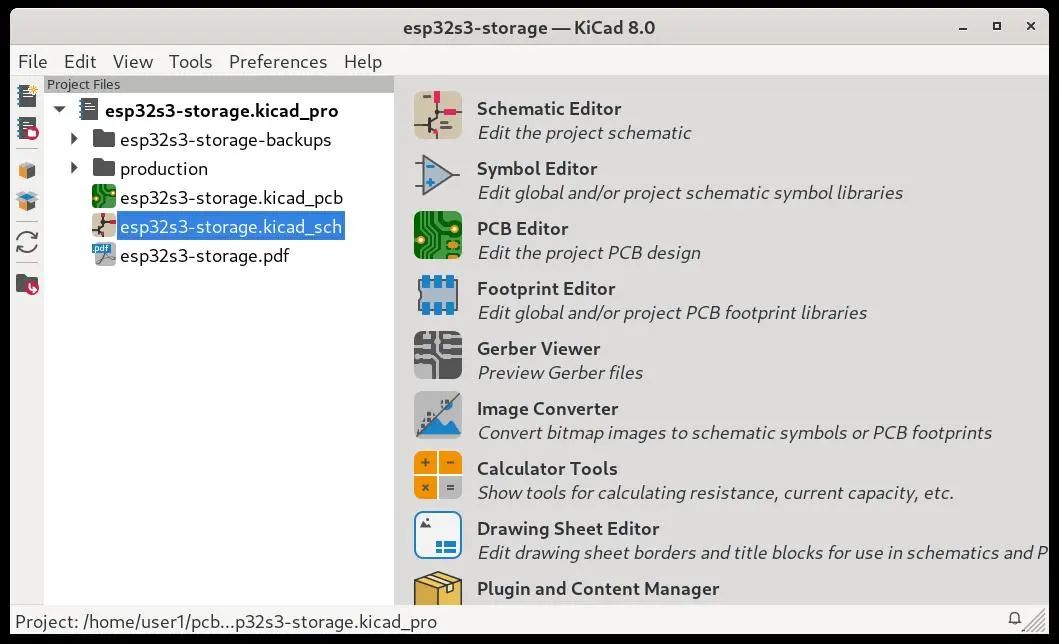
Below is the main interface of KiCad 8, where I create projects. I created a project called esp32s3-storage, and in the left file list, you can see esp32s3-storage.kicad_sch and esp32s3-storage.kicad_pcb, which represent the circuit schematic and PCB circuit diagram, respectively.
Circuit Schematic
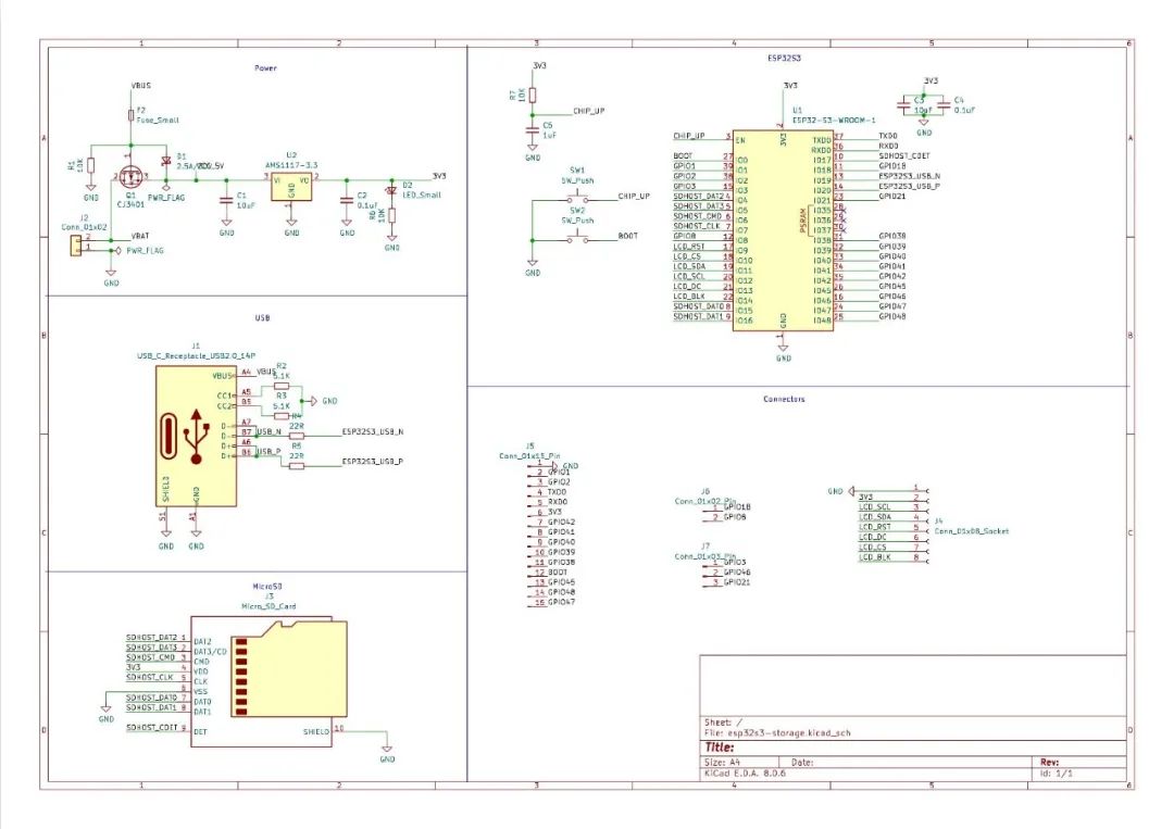
The current circuit schematic is still relatively simple, divided into five parts: power supply, USB interface, MicroSD card, ESP32S3 chip, and various connectors. After connecting all the components, I achieved a small system based on ESP32S3 that supports USB or battery power supply with an SPI display interface and a MicroSD card slot. The final circuit diagram looks like this.
PCB Circuit Diagram
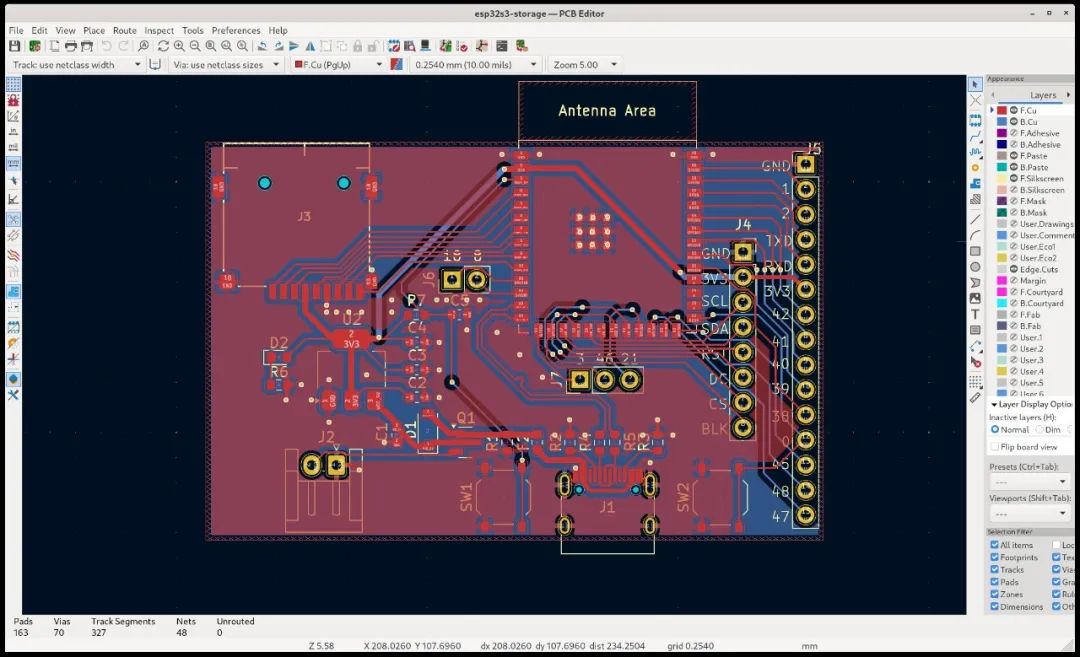
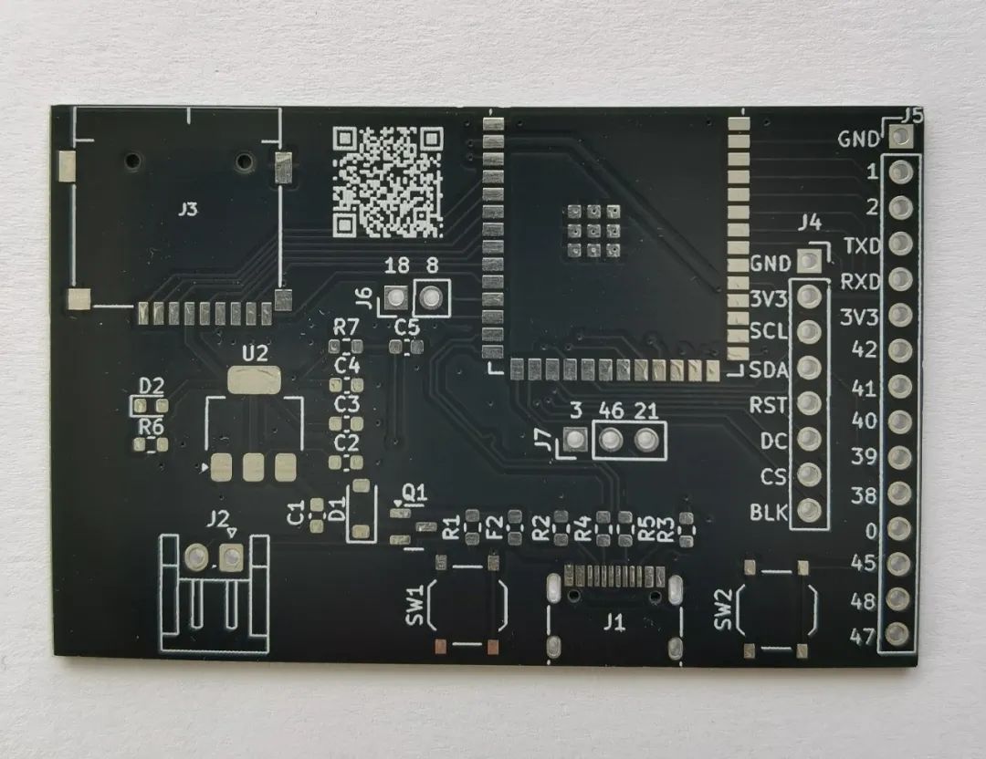
After completing the schematic, I can draw the PCB circuit diagram once the component packages are determined. The image below is the final drawn PCB circuit. The red and blue lines in the image are the wires connecting electronic components, and the labeled areas indicate the positions of the components. The top right corner U1 is the ESP32S3, the bottom right corner J1 is the USB-C interface, the top left corner J3 is the position for the MicroSD card, and the bottom left corner J2 is the 5V battery input interface. There are two rows of interfaces on the right edge; the long ones are the GPIO ports that have not been assigned yet, and the shorter ones are for connecting the SPI interface display module. Additionally, there are two shorter GPIO interfaces located in the middle of the board. The remaining board area is filled with GND areas, hoping to ensure signal stability.
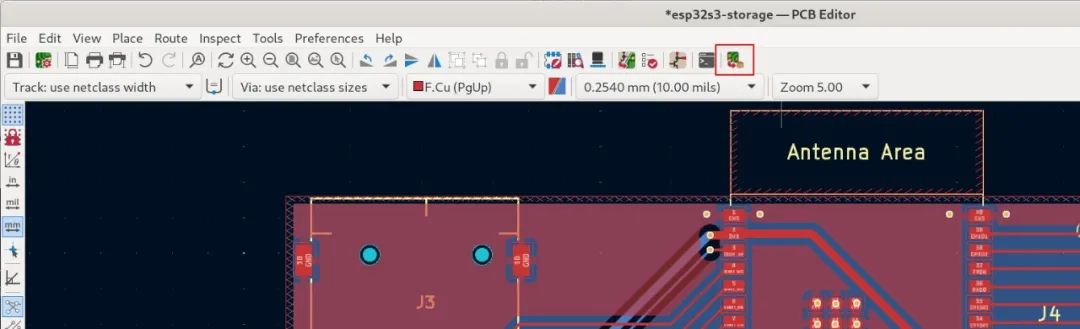
After finalizing the PCB circuit diagram, I generated the Gerber files using the Fabrication Toolkit plugin (which can be installed through the Plugin and Content Manager by searching directly) to submit to the PCB manufacturer for PCB production.
Conclusion
The circuit schematic and PCB files in this article can be downloaded fromesp32s3-storage. The efficiency of the PCB manufacturer is very high; my short article was not even finished, and the completed PCB had already arrived. The finished product looks like this; besides the black paint layer, doesn’t it look quite similar to what was shown in KiCad 8? The next step is to solder the board and conduct tests; I will report back with progress.
Links
-
1.esp32s3-storage – https://github.com/paul356/esp32s3-storage