Chapter 13
CGC – Clock Control
Accompanying Video Introduction
“16-CGC Clock Control (Section 1) – Clock Source”
https://www.bilibili.com/video/BV1yH4y1z7PZ/
“17-CGC Clock Control (Section 2) – Clock Block Configuration Analysis”
https://www.bilibili.com/video/BV1334y1c7nd/
“18-CGC Clock Control (Section 3) – Clock Configuration and Output Experiment”
https://www.bilibili.com/video/BV1rQ4y1x7AT/
CGC
CGC (Clock Generation Circuit): Clock Generation Circuit
13.1
Introduction to the CGC Module
#CGC stands for Clock Generation Circuit, which can also be referred to as the “Clock Control Circuit”.
13.1.1
Clock Source
As we learned in “Digital Logic Circuits”, in a chip integrated circuit system, a clock signal must be input to drive the logic circuits to function properly. So where do these clock signals come from?
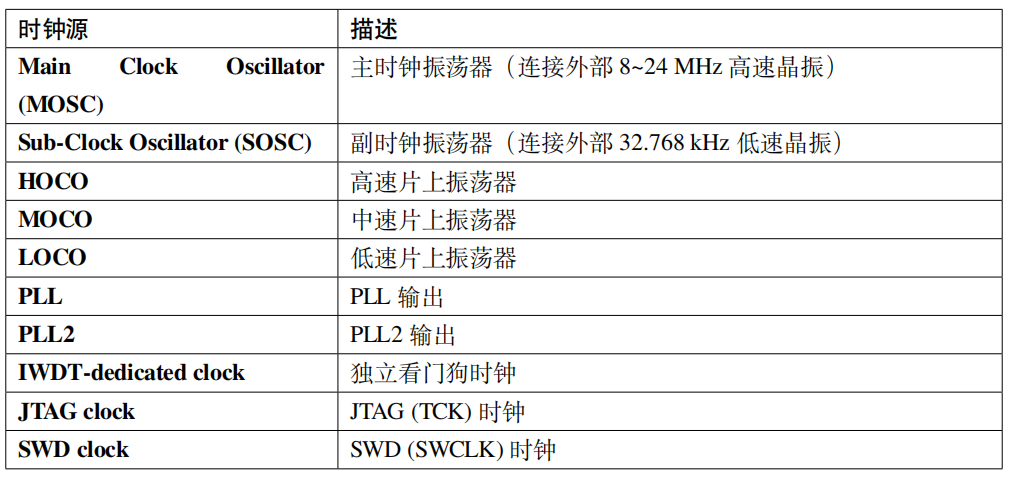
The source of the clock signals is referred to as the clock source. The clock sources for RA6M5/RA4M2 are shown in the table below:
Table 1: RA6M5/RA4M2 Clock Sources
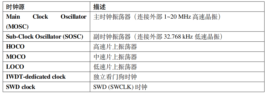
The clock source for RA2L1 is shown in the table below:
Table 2: RA2L1 Clock Sources
Detailed explanation of related concepts:
Main Clock Oscillator (MOSC):
Main Clock Oscillator
-
RA6M5/RA4M2 connects to an external 8 ~ 24 MHz high-speed crystal oscillator (connected to pins EXTAL, XTAL);
-
RA2L1 connects to an external 1 ~ 20 MHz high-speed crystal oscillator (connected to pins EXTAL, XTAL).
Sub-Clock Oscillator (SOSC):
Sub Clock Oscillator
-
Connects to an external 32.768 kHz low-speed crystal oscillator (connected to pins XCIN, XCOUT).
-
The external clock frequency of 32.768 kHz is generally used for RTC to provide time and calendar functions for the user system.
Phase Locked Loop (PLL, PLL2):
PLL stands for Phase Locked Loop.
The PLL circuit has the function of multiplying the oscillator frequency, allowing selection of the input clock signal to the PLL, and performing division and multiplication. The input clock sources can be MOSC or HOCO, with input frequencies ranging from 8 MHz to 24 MHz, and the multiplication ratio can be selected between 10 and 30 (0.5 step).
-
PLL output frequency: 120 MHz ~ 200 MHz.
-
PLL2 output frequency: 120 MHz ~ 240 MHz.
-
Note:RA2L1 does not have a PLL, so its main frequency (48 MHz) is relatively low, which is also beneficial for low power consumption.
High-speed on-chip oscillator
(HOCO):High-speed On-chip Oscillator
-
Oscillation frequency: 16/18/20 MHz for RA6M5/RA4M2
-
Oscillation frequency: 24/32/48/64 MHz for RA2L1
Middle-speed on-chip oscillator
(MOCO):Middle-speed On-chip Oscillator
-
Oscillation frequency: 8 MHz
Low-speed on-chip oscillator
(LOCO):Low-speed On-chip Oscillator
-
Oscillation frequency: 32.768 kHz
IWDT-dedicated clock (IWDTLOCO):
IWDT Dedicated On-chip Oscillator
-
Oscillation frequency: 15 kHz
External clock input for JTAG (TCK):
External Clock Input for JTAG
-
Oscillation frequency: maximum 25 MHz
-
Note:RA2L1 does not support the JTAG interface.
External clock input for SWD
(SWCLK):External Clock Input for SWD
-
Oscillation frequency: maximum 25 MHz for RA6M5/RA4M2
-
Oscillation frequency: maximum 12.5 MHz for RA2L1
13.1.2
Module Input Clock
From the above, we know that there are various clock sources input, and these clock sources need to output clock signals to various clock lines, while the various modules of the chip are connected to these clock lines.
Each module in the system requires different operating frequencies, corresponding to the maximum clock frequencies that each clock line can provide, which are not all the same. Users need to particularly consider the input clock frequency when using certain peripherals or modules, which can be satisfied by configuring the clock frequency of the corresponding clock line to meet the needs of different modules.
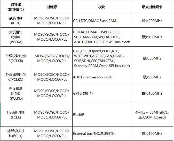
Taking RA6M5 as an example, below is the clock source and the maximum frequency it can provide for the main internal clock lines of the system.
Table 3: RA6M5 Internal Clock Description
Note some limitations when setting clock frequencies:
-
ICLK ≥ PCLKA ≥ PCLKB, PCLKD ≥ PCLKA ≥ PCLKB
-
ICLK ≥ FCLK, ICLK ≥ BCLK
13.1.3
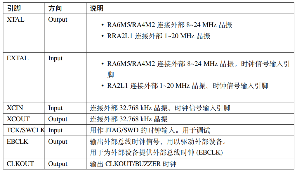
Clock-related Pins
The clock-related pins and their descriptions are shown in the table below.
Table 4: Clock-related Pins

Need Technical Support?
If you have any questions while using Renesas MCU/MPU products, you can scan the QR code below or copy the URL into your browser to access theRenesas Technical Forum for answers or online technical support.
https://community-ja.renesas.com/zh/forums-groups/mcu-mpu/
To be continued
Recommended Reading
Key_Scan Key Scanning Function – Renesas RA Series FSP Library Development Practical Guide (26)
FSP Library Startup File Detailed Explanation – Renesas RA Series FSP Library Development Practical Guide (27)
SystemInit() – Renesas RA Series FSP Library Development Practical Guide (28)