With the rapid development of manufacturing processes, the complexity of miniaturized devices is increasing day by day. In cutting-edge industries such as microelectronics, medical technology, and photonics, micro-devices often adopt multilayer stacked structures made of different materials to meet increasingly complex multifunctional requirements.
Especially in the healthcare sector, the application of Continuous Glucose Monitoring (CGM) systems has brought breakthrough advancements for diabetes patients. It can provide real-time blood glucose data, significantly enhancing the efficiency and effectiveness of patients managing their blood glucose levels. However, the manufacturing process of CGM sensors is extremely complex and demanding. Since the sensors need to be implanted subcutaneously for long periods and come into contact with bodily fluids, their biocompatibility, micro-nano precision, and long-term durability are crucial. Taking the processing of the platinum-iridium alloy needle sensor, a key component of CGM, as an example: it requires precise etching of specific areas of the PI (polyimide) coating at the micron scale through a precision subtractive manufacturing process, leaving only the necessary electrode areas.
 PART 01Why Remove the PI Coating?
The base layer of this CGM sensor probe, with a cross-sectional diameter of only 0.19mm, is made of platinum-iridium alloy (Pt/Ir), which is an ideal choice for such precision medical implants due to its extremely high inertness, biocompatibility, excellent corrosion resistance, lower impedance, and higher charge transfer capability. The surface is coated with polyimide (PI), which has extremely low leakage and excellent dielectric properties, widely used as a protective and insulating layer for platinum-iridium alloy electrodes.
To enable the probe to accurately sense blood glucose signals and efficiently react electrochemically with interstitial fluid, specific areas of the platinum-iridium alloy must be precisely exposed to form clear conductive pathways and sensing interfaces. Therefore, selectively and accurately removing the PI coating while preserving the functional characteristics of the underlying platinum-iridium alloy is key to ensuring the core functionality of the CGM probe and is one of the main challenges in its manufacturing process.
PART 02Does Femtosecond Laser Damage the Platinum-Iridium Alloy Surface?
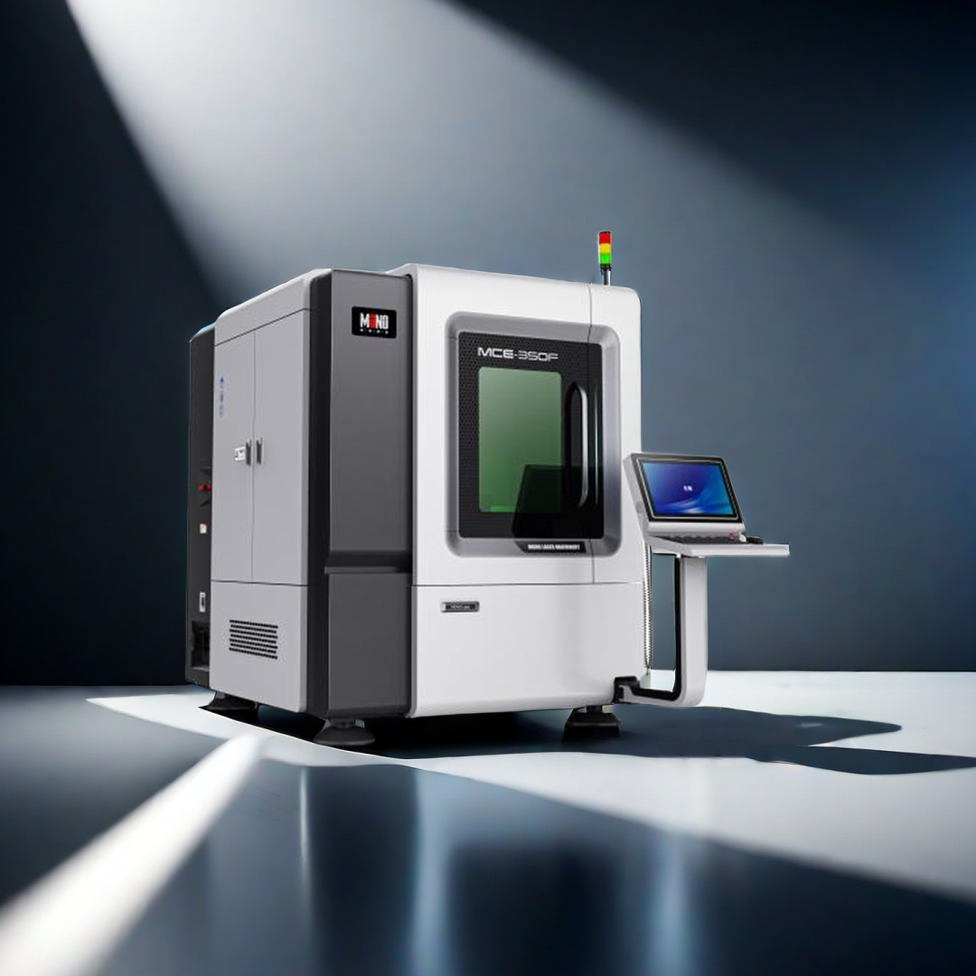
Faced with the potential limitations of traditional techniques, the monochrome technology femtosecond laser depth etching technology, with its process advantages and high-quality processing effects, has brought revolutionary breakthroughs for “coating removal” micro-nano processing needs, especially in the manufacturing of complex curved devices. It can be seen as a powerful supplement or a better choice to existing processes.

Monochrome Technology Case: Etching depth of 0.05mm, accuracy ±1μm
1. Precise Depth Etching, Protecting the Underlying Material, Achieving High-Quality Surface
The femtosecond laser precision etching equipment removes material using ultra-short pulse energy (femtosecond level), where energy is instantaneously absorbed and vaporized at the material surface, almost without generating heat that diffuses to the surroundings (especially to the underlying platinum-iridium alloy substrate). The femtosecond laser depth etching technology can control the etching depth with extremely high precision (accuracy ≤ ±1μm, minimum etching depth ≤ 0.1μm), ensuring that the PI coating is accurately removed to the predetermined depth while the underlying platinum-iridium alloy surface is almost undamaged. It is compatible with metals, non-metals, and composite materials, with a wide range of applicable materials.
Thanks to the ultra-fine light spot and control system, the processed platinum-iridium alloy surface can achieve a nanometer-level roughness (Ra < 0.2μm). An ultra-smooth surface is crucial for medical implants like CGM probes that need to have good contact with biological tissues, reduce friction, and ensure stable electrochemical signal transmission.

2. Overcoming the “Seam” Challenge on Curved Surfaces, Achieving High Consistency
Patterning processing on larger curved surfaces and achieving high-quality surfaces is difficult for traditional processes, and segmented processing methods easily produce “seams” and leave metal residues, leading to circuit connectivity or functional failure. Femtosecond laser precision etching equipment supports large-size processing ranges, with splicing accuracy ≤ ±1μm, achieving seamless splicing on curved and complex surfaces or minimizing the impact of seams, ensuring the functional integrity and electrical performance of microstructures.
 PART 03Comparison with Traditional ProcessesCoating removal technologies, such as chemical stripping, thermal stripping, and plasma etching, often face insurmountable obstacles when applied to high-precision, high-value devices:
· Chemical stripping: Difficult to achieve micron-level precise control, chemical solvents may corrode or alter the surface properties of the underlying material, and residue handling is complex.
· Thermal stripping/traditional laser ablation: Generates significant heat-affected zones, easily leading to molten residues, edge carbonization, and severe thermal damage.
· Plasma etching: Complex processes and expensive equipment, with high maintenance difficulty, more suitable for large-scale manufacturing.
PART 04Conclusion
The femtosecond laser etching technology, with its excellent processing performance and broad application potential, not only provides solid technical support for the innovation and breakthroughs of future implantable medical devices but will also strongly promote the development of “extreme manufacturing” in the field of miniaturized, high-precision device manufacturing.
