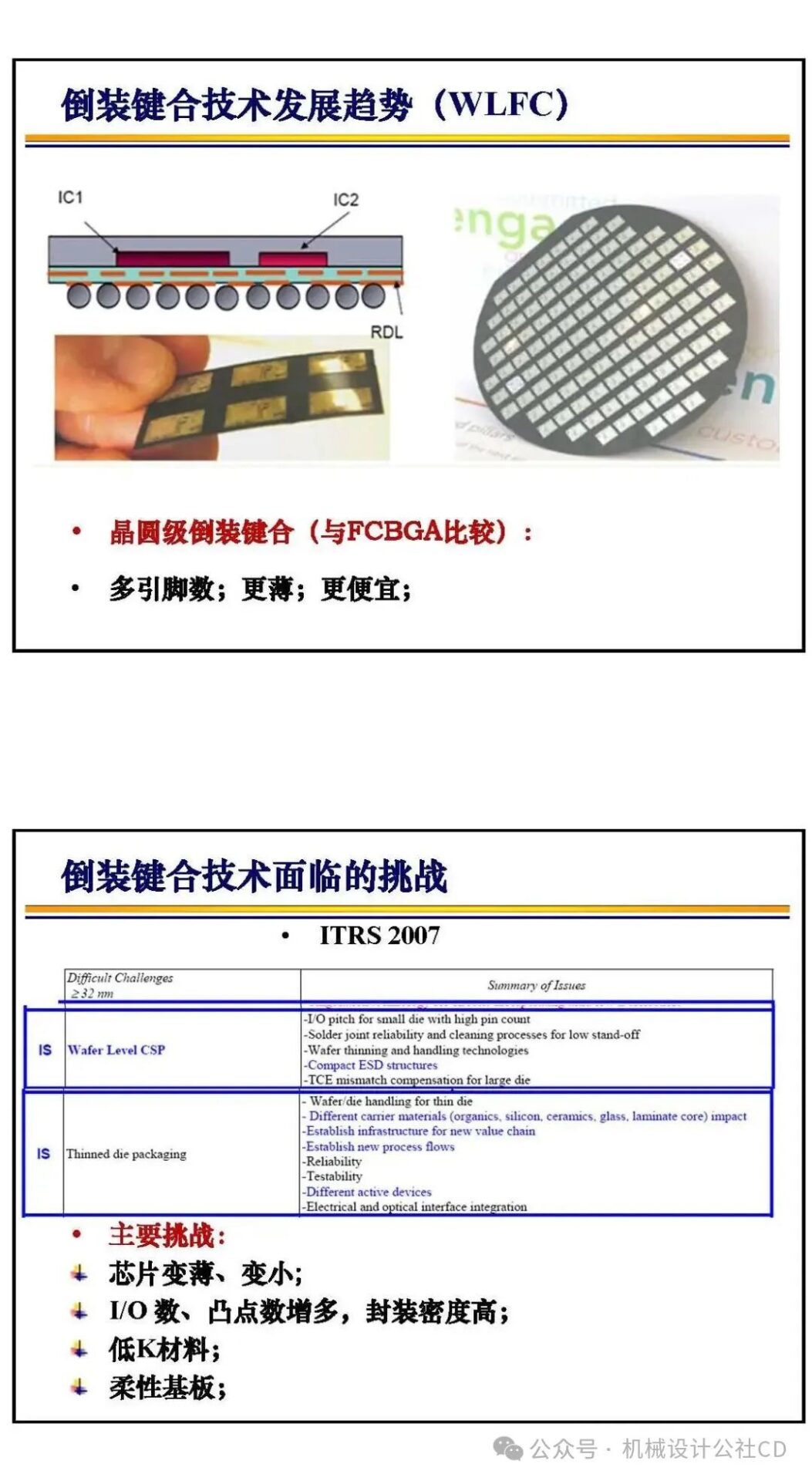
The bonding technology in chip manufacturing is a crucial part of the semiconductor manufacturing process. It connects different materials securely through physical or chemical methods, achieving electrical and mechanical connections in integrated circuits. There are various types and applications of bonding technology in chip manufacturing, each with its unique advantages and applicable scenarios.
Types and Principles of Bonding Technology
-
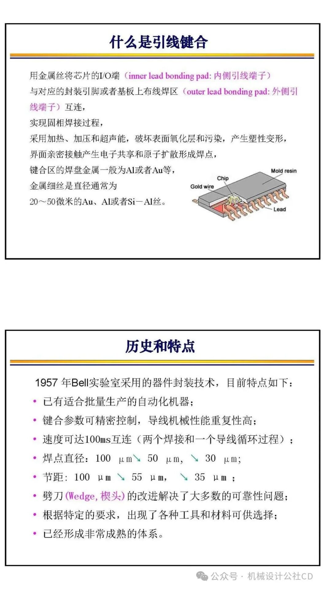
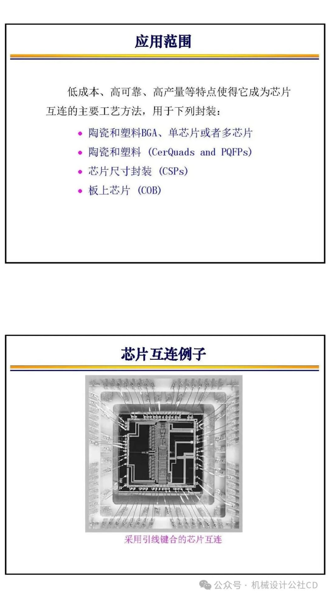
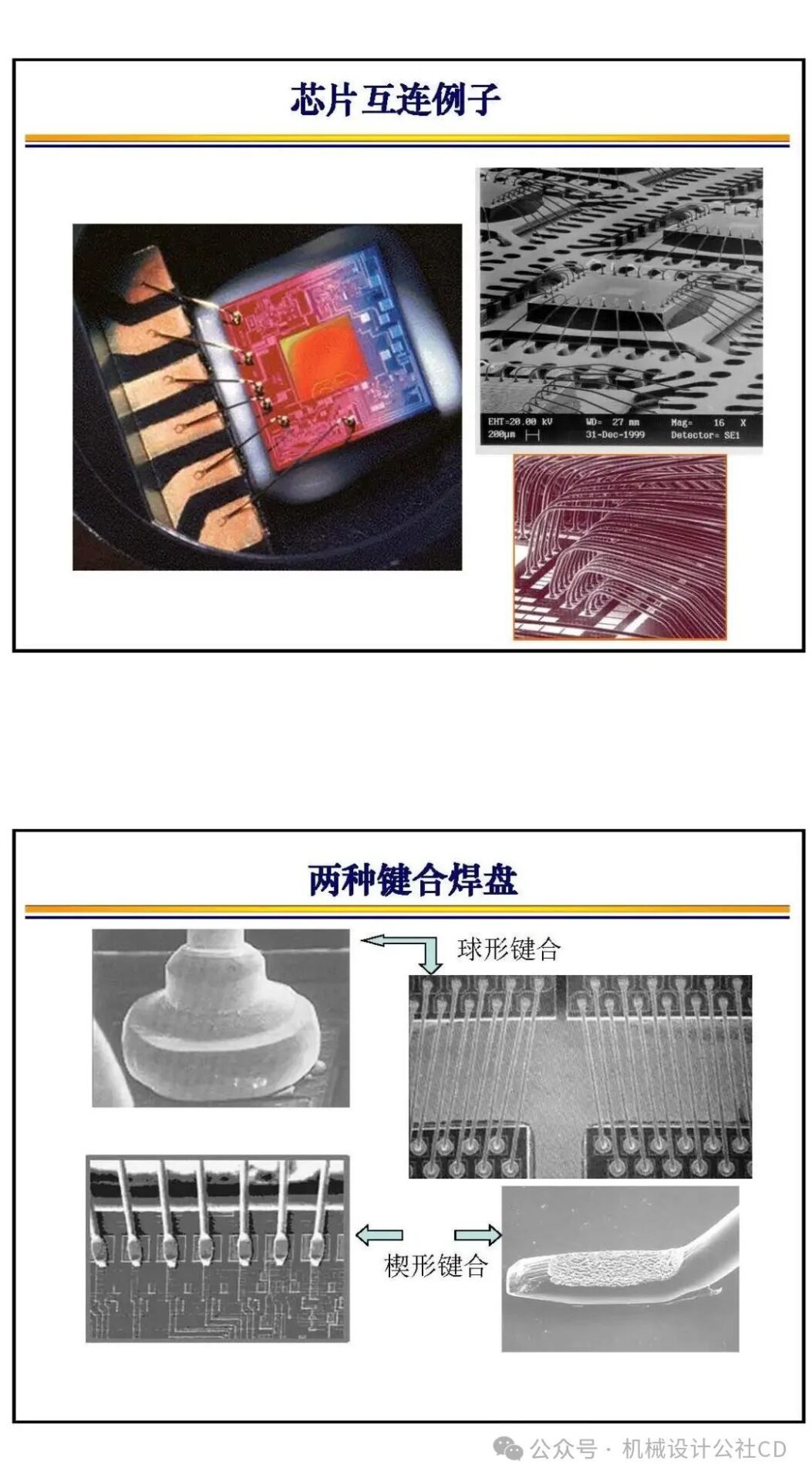
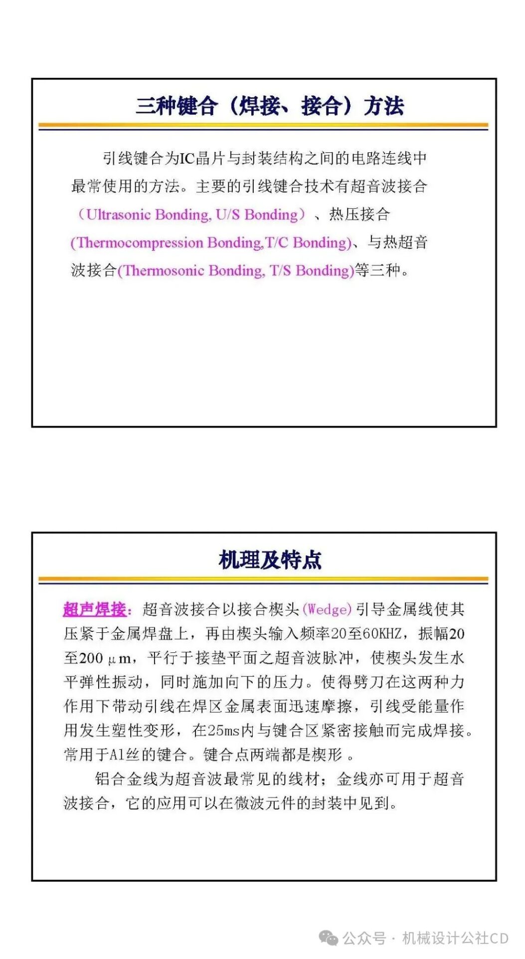
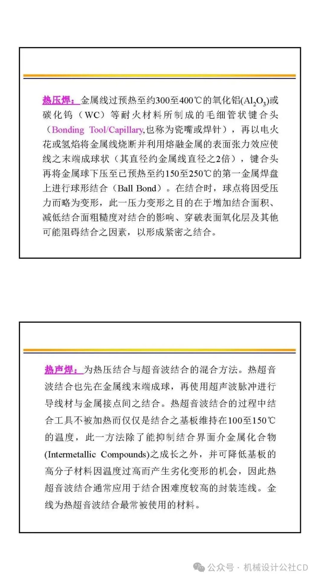
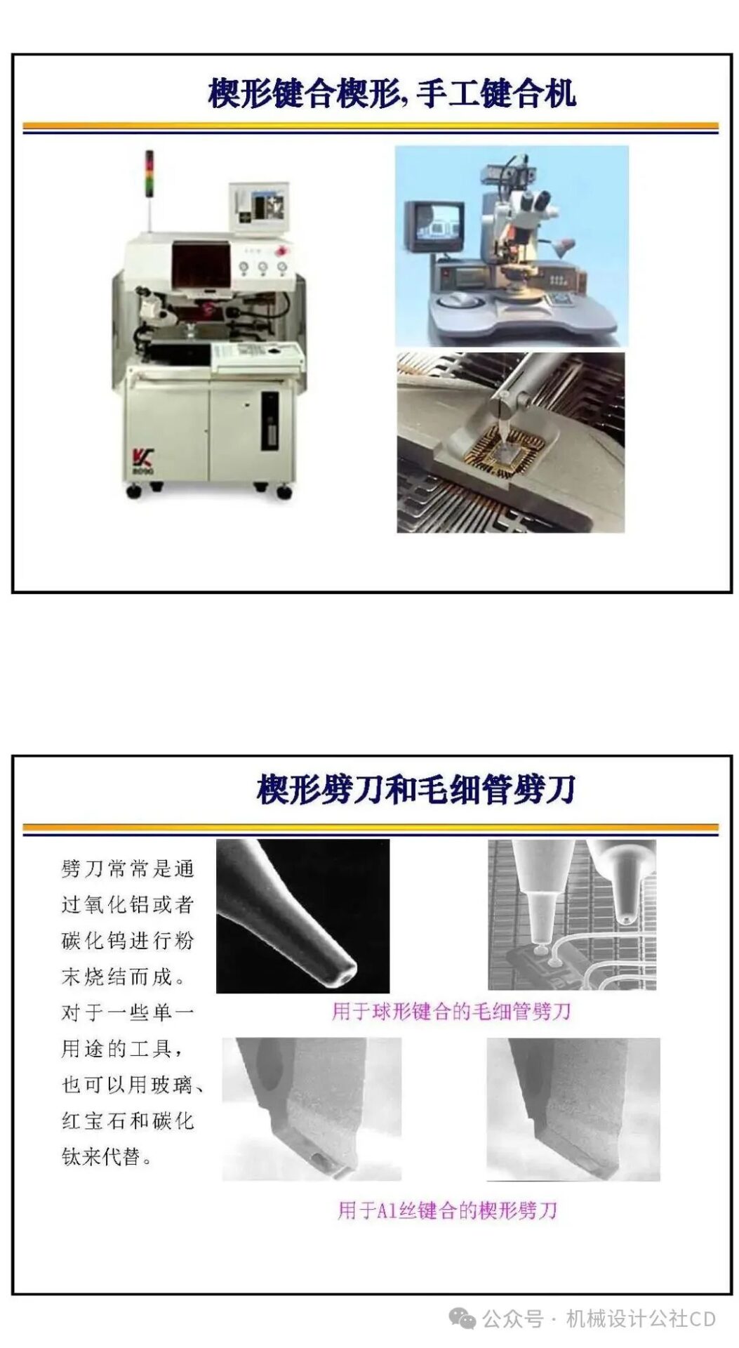
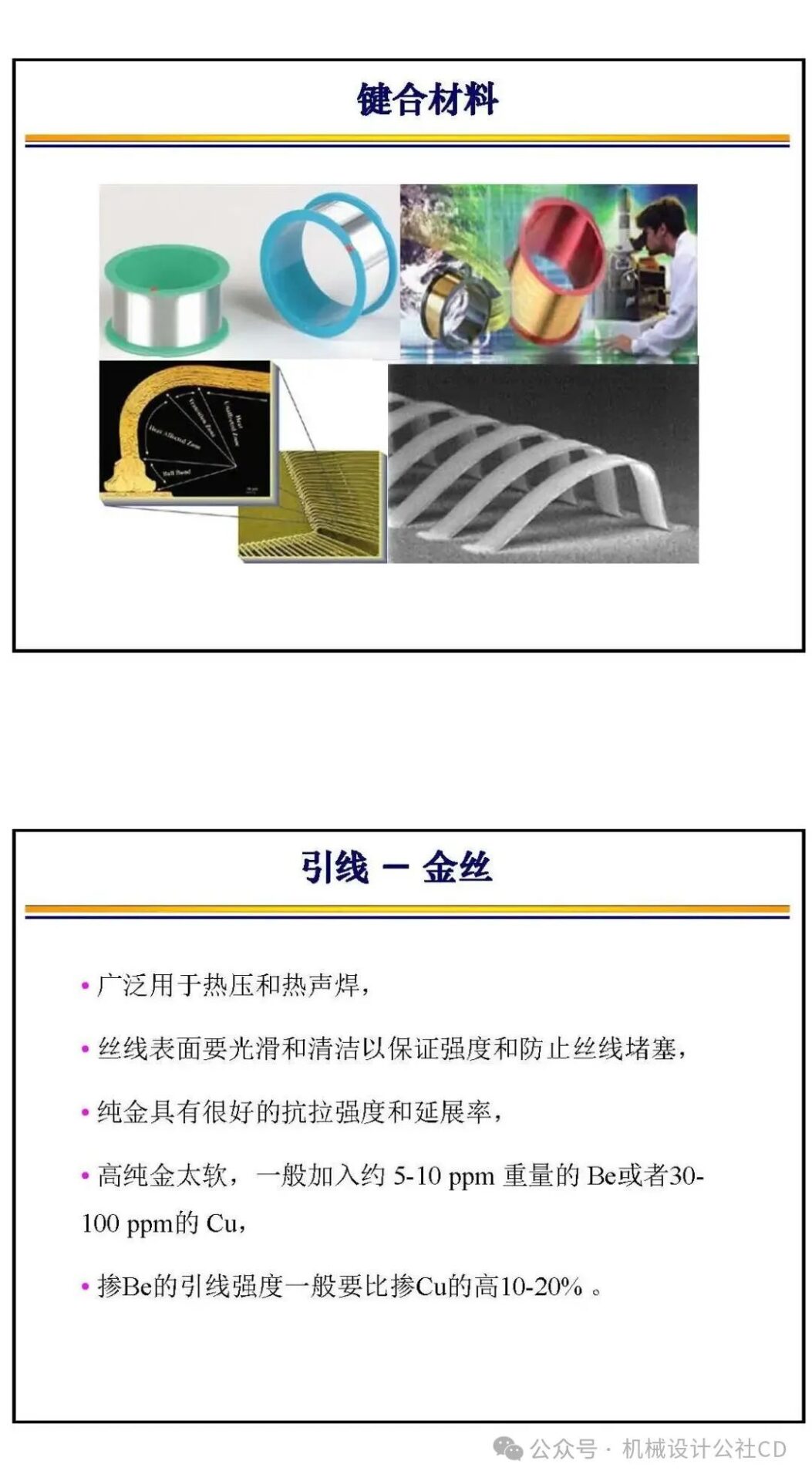
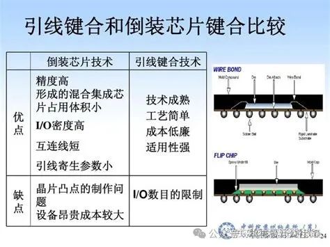
Wire Bonding: Wire bonding is one of the most traditional bonding methods, connecting the chip’s electrode leads to external circuits using metal wires. This method is cost-effective but has limited signal density and connection speed, thus restricting its application in compact devices.
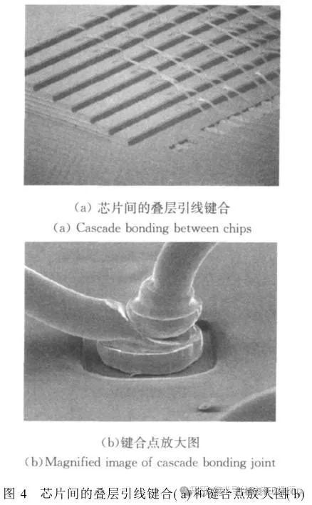
Wire bonding technology in 3D packaging
-
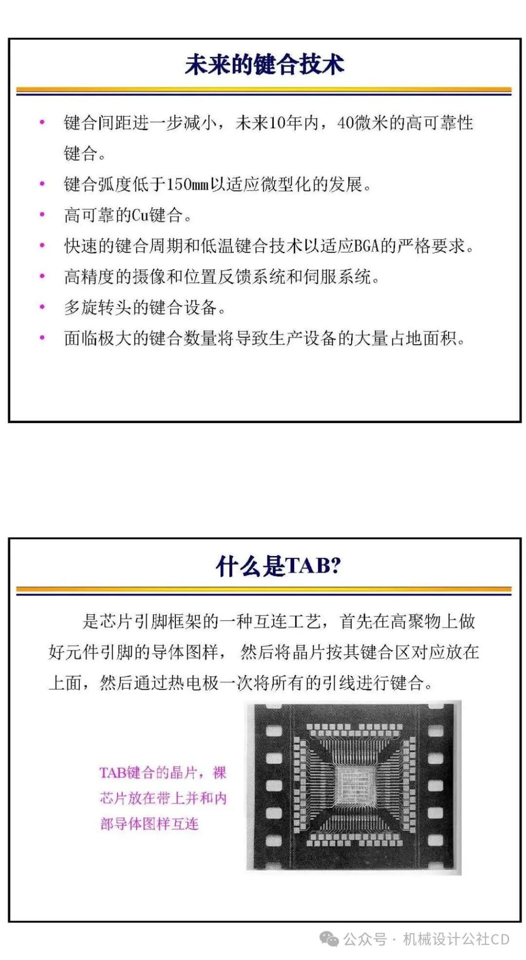
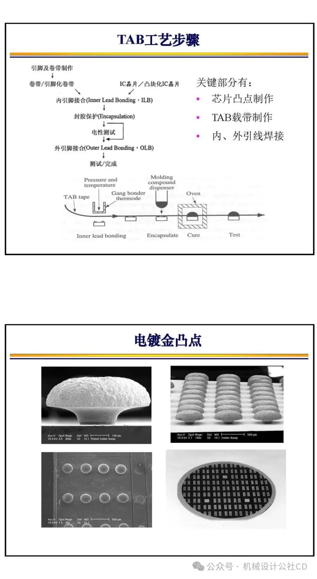
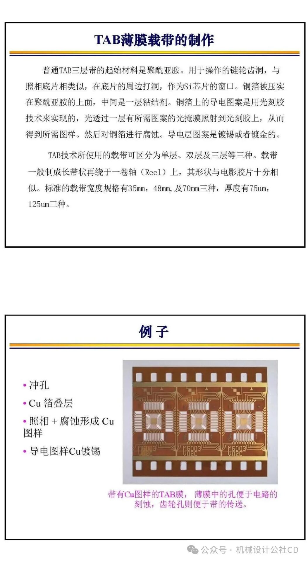
Tape Automated Bonding (TAB): With technological advancements, TAB has been introduced to meet the demands of high-density, ultra-thin, and small-sized chips. The TAB technology includes steps such as bump formation on the chip soldering area, tape lead fabrication, inner lead welding, substrate bonding, and outer lead welding.
-
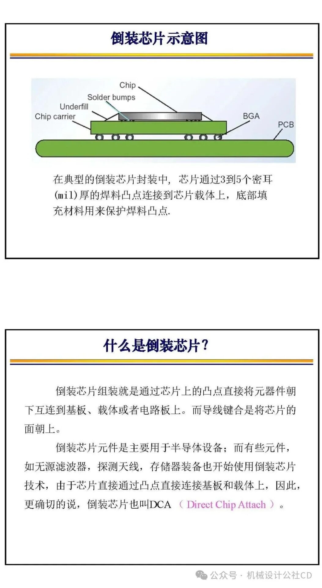
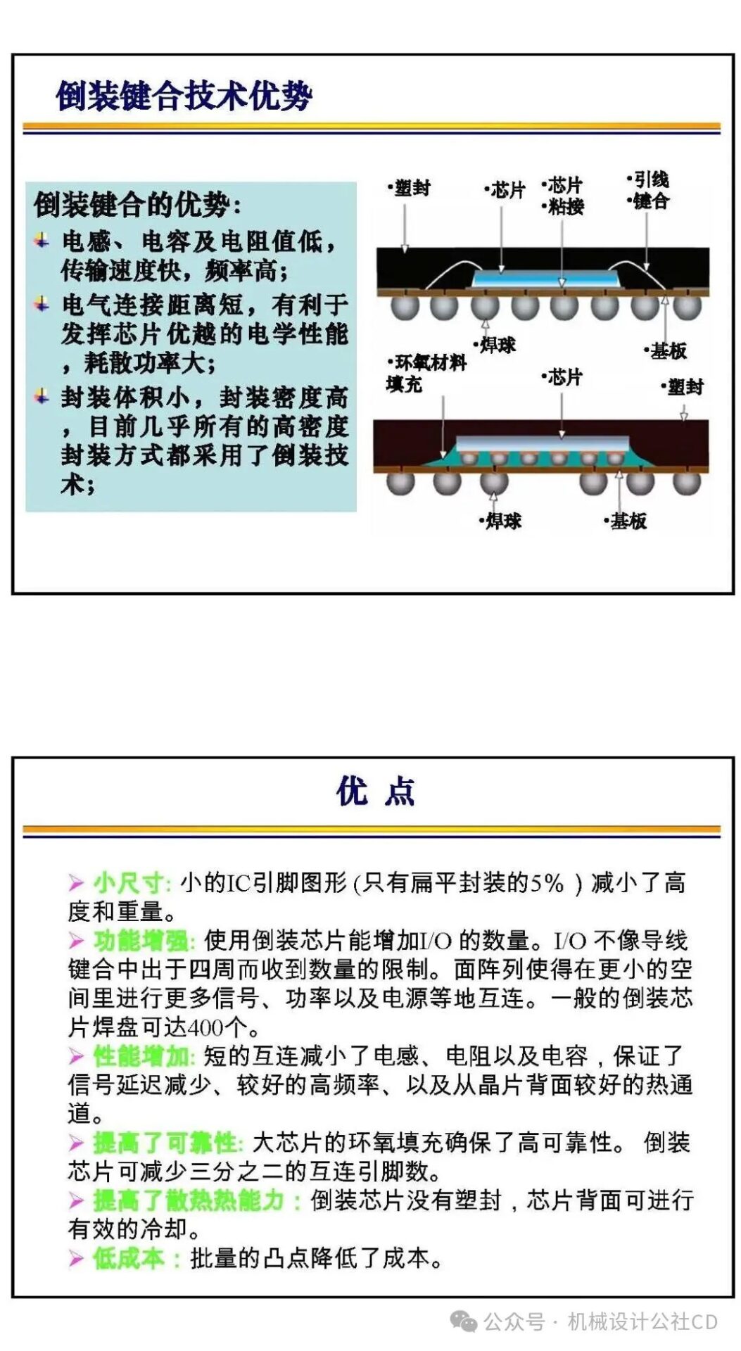
Flip Chip Bonding: Flip chip bonding involves flipping the chip and attaching it directly to the substrate, achieving better electrical performance and higher reliability. This method allows for more electrical connections and reduces signal delay.
-
Hybrid Bonding: Hybrid bonding combines the advantages of direct and indirect bonding by using metal layers or interface materials to enhance bonding strength and reliability. For example, Cu/SiO2 hybrid bonding utilizes covalent bonds between Cu and SiO2 to improve bonding reliability and adaptability.
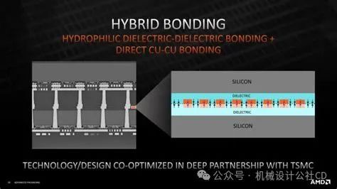
AMD’s design towards multilayer small chips
-
Direct Bonding: Direct bonding technology forms strong chemical bonds between the surfaces to be bonded without the need for an intermediate layer. This method can lower bonding temperatures and reduce the effects of thermal mismatch, making it suitable for high-precision and high-reliability applications.
-
Metal Bonding: Metal bonding includes methods such as eutectic bonding and thermocompression bonding. For instance, Cu-Sn alloys have good processability and scalability at low temperatures, while thermocompression bonding forms a strong metal bonding interface through solid-state diffusion.
-
Dielectric Bonding: Dielectric bonding technology utilizes polymer adhesives or oxide layers for connections, such as epoxy resins and polyimides, which are widely used in 3D packaging due to their low bubble formation, high electric field strength, and good chemical stability.