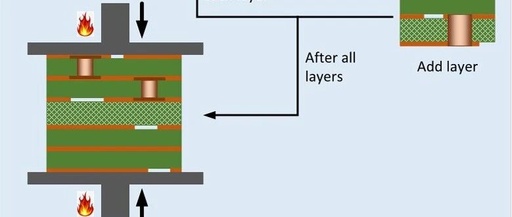
PCB Warpage Control Solutions (Supplement)
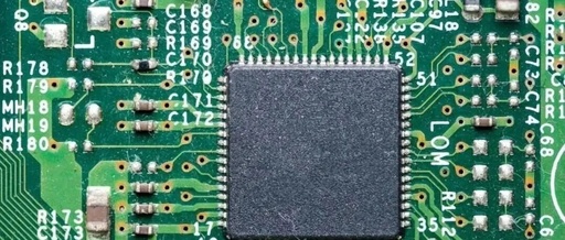
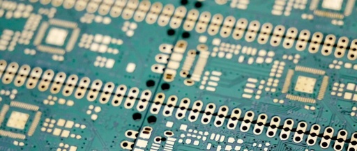
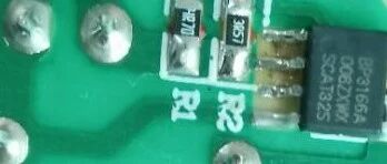
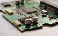
PCB warpage is very common during the production and processing of PCBs. Once it occurs, it can seriously affect the performance and reliability of the product, such as poor soldering and component damage. How can we effectively control PCB warpage? First, we need to understand 1. Standards for PCB Warpage According to IPC standards, the … Read more