

Source: https://zhuanlan.zhihu.com/p/468286383
RTOS is widely used in projects, and to better understand how RTOS works, one needs to know the general process of CPU operation.
Why Use RTOS?
Why use RTOS when bare metal programming works fine? When starting with microcontrollers, one typically writes a while loop in the main function and adds the necessary code within that loop to achieve the desired functionality.
As long as it runs, the code is fine; this method is commonly referred to as “bare metal coding”. For example, if the while loop needs to control four motors to rotate at different angles while displaying the specific angles on an OLED screen, the bare metal execution would involve all four motors rotating and then sending data to the OLED screen (or sending one data point at a time to the OLED screen).
We know that the principle behind motor rotation involves adjusting the duty cycle of the PWM signal. This means that when PWM is activated, it requires a delay; thus, the last motor must wait until the previous motors have completed their tasks before it can run. This introduces delays, leading to the question: is there a way for all motors to run simultaneously? This is where RTOS comes into play.
Of course, for overly simple programs like turning on a single light, RTOS is unnecessary; bare metal programming is sufficient. RTOS is primarily aimed at multi-tasking programs.
To better understand how RTOS works, one must know the general process of CPU operation:
CPU
The Central Processing Unit (CPU) is one of the main components of a computer, primarily responsible for interpreting computer instructions and processing data calculations in software.
The introduction mentions that the CPU’s function involves instruction processing and data calculations, so the CPU must have both computational and instruction analysis components.
ALU (Arithmetic Logic Unit)
The ALU within the CPU is primarily responsible for processing data. Its conceptual diagram is shown below.
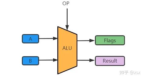
The primary function of the logic unit is logical operations. In the CPU, the ALU is responsible for all logical operations. The ALU consists of several components. For example, in the case of A+B=C:
-
• Input Data: An operation requires at least two operands, so the ALU’s input consists of two operands (A and B as shown in the diagram).
-
• Operation (OP): The operation instruction determines what operation to perform on operands A and B, whether it is addition, subtraction, multiplication, division, or a combination.
-
• Output Result: The result of the operation is output.
-
• Flags: What is the purpose of flags? For example, if we are performing the operation A+B, and if the CPU operates on 16 bits, the maximum value for two numbers is 15. If A=10 and B=6, A+B exceeds the ALU’s calculation range. To handle overflow, the ALU generates an Overflow flag and stores the excess in a register for the next input. Furthermore, the ALU can also compare the sizes of two operands. For instance, if A=10 and B=6, and the operation is to compare A and B, the operation would use subtraction. The result of A-B would generate a flag (0 or 1) indicating the size comparison.
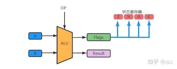
From the above, we can see that the ALU’s output is stored in a register group (it can also be stored in RAM). But where are the flags stored?
The flags generated by the ALU are typically stored in a special register called the Program Status Register (PSR). Each instruction executed updates the corresponding status bits, and different instructions affect different status bits, which need to be checked in the chip manual.
What status does the PSR store? Despite various chips having their types of flags, every chip must have at least the following flags:
-
• Z (Zero) Flag: If A-B=0, a zero flag is generated.
-
• N (Negative) Flag: A negative result.
-
• O (Overflow) Flag: If A+B=16>15, an overflow flag is generated.
-
• C (Carry) Flag.
Data Storage
We know that the ALU requires two operands as input; where do these operands come from?
There are several sources for the ALU’s operands:
Internal Registers
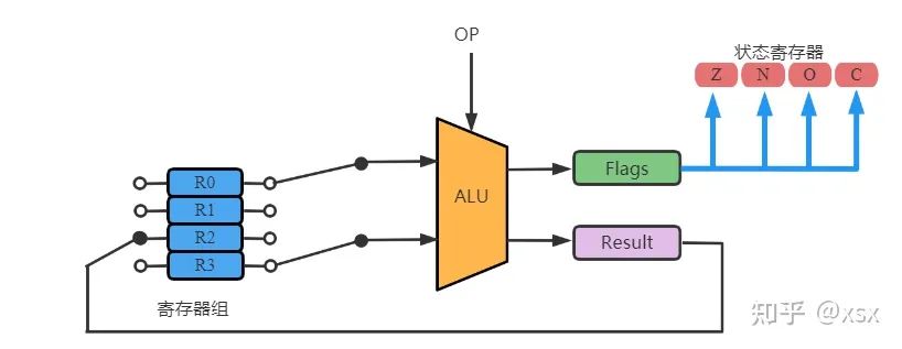
When designing a CPU, several internal registers are created to implement temporary storage. The properties of registers are as follows:
-
• Used to temporarily store/retrieve operands. For example, the ALU’s input data can come from the CPU’s general register group, and the ALU’s output can also be stored in registers (note that the internal register storage is temporary).
-
• Every CPU contains several general/special registers.
-
• The data and width of registers are important metrics for measuring a CPU.
For internal CPU registers, they can be compared to scratch paper during an exam. Each intermediate result can be written on scratch paper (the output of the ALU), and the intermediate results can be used as input for further calculations (providing input operands for the ALU). Once the final result is calculated, it is filled in on the exam paper (the final result must be stored in external memory).
External Memory
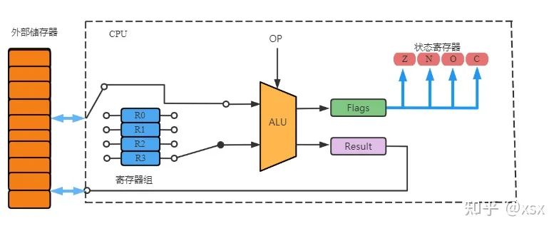
What is stored in external memory? As mentioned, internal registers temporarily store data (like scratch paper), while the final submission is the exam paper (comparable to external storage for the main content of the program). If the entire CPU operation process is likened to a math exam, then the ALU’s function is to help us calculate the results. Where do the data A and B originate?
They come from the exam paper. The exam questions require us to calculate the result of A+B, which is what the exam requires us to do (the requirement is the instruction the CPU must execute). After calculating on scratch paper, the result is written on the exam paper (this process is referred to as “storing data on the exam paper”). Similarly, the ALU’s output is stored in external memory. Thus, external storage contains:
-
• Instructions executed by the CPU.
-
• Data saved during CPU operation.
CPU Instructions
Similarly, using the exam paper as an example, there is a question on the paper: A=1, B=1, what is the value of A+B and C? When you see the question, you calculate the result based on the question’s “requirement”. Similarly, the CPU needs someone to give it questions (the user). The user’s code is processed by the compiler, converting the program into machine code instructions (the CPU’s exam paper). Once the instructions are compiled, they are stored and then handed to the CPU for execution (just like a teacher sealing the exam papers for storage).
CPU Data
We have established that external memory stores the results of ALU calculations (writing the results from scratch paper to the exam paper) and that the memory can also store temporary data.
Is there a conflict between the temporary data storage in the internal registers and external memory?
The temporary storage times differ; since internal registers are located within the CPU, data retrieval from them is the fastest. Therefore, frequently accessed data should ideally be stored in the internal general registers. However, for data that is accessed infrequently, it should be stored in external memory. This is not absolute; users can choose to optimize compilation to store frequently accessed data in external memory, but this approach will significantly reduce data processing speed.
Fetching Instructions
How does the CPU fetch instructions from external memory?
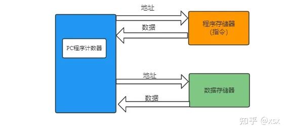
As previously mentioned, when the teacher has finished preparing the exam papers, if they find that one paper is missing, they might decide to write a new paper on the board. The students then have to solve the problem presented on the board. Similarly, the CPU needs a “blackboard” to store these instructions. In the CPU, this blackboard is represented by the Program Counter (PC), which stores the address of the next instruction rather than the instruction itself.
Program Counter
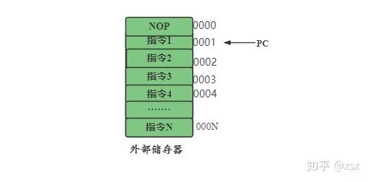
The Program Counter (PC) is a special register within the CPU that always points to the address of the next instruction. As shown in the diagram, external memory is made up of several boxes, each with an address number, and each box stores the instruction the CPU needs to execute. The PC always points to the address of the next instruction. If the current instruction is NOP, the address pointed to by the PC is 0001.
Why does the PC always point to the next instruction rather than the current instruction?
If the external memory is filled with data, and the PC points to the top (where overflow might occur), there could be unpredictable errors. By pointing to the next address, if the data happens to fill the top, the CPU can set the PC to point to an exception to provide feedback.
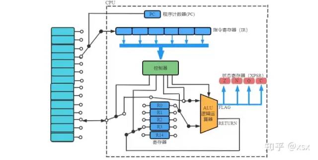
With the PC register, instructions from memory can be fetched. As shown in the diagram, under the guidance of the PC, the instructions stored in memory are loaded into the instruction register. After parsing the instruction, the data is handed to the control unit, which loads data from memory and determines what operations the ALU will perform, etc. The PC register is a crucial mechanism in program execution. We can further deepen our understanding of it through the stack.
Memory
We know that the instructions and data for the CPU come from external memory. The CPU’s memory can be classified as follows:
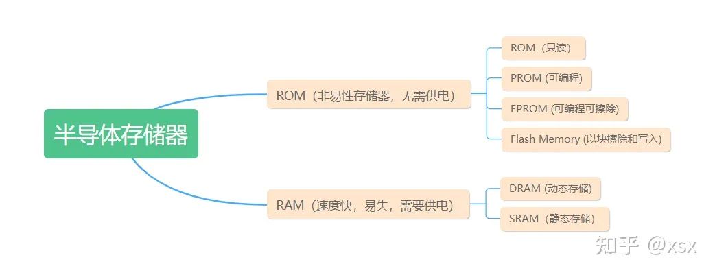
ROM (Read-Only Memory)
ROM can only be read, not written. Once information is written, it becomes fixed and cannot be lost even if the power is cut off; hence, it is also known as fixed storage. In microcontrollers, the first instruction executed by the CPU upon power-up is fetched from ROM. What content does the CPU read from ROM during the power-up process?
-
• Allocate address space for global variables: The initial values are copied from ROM to RAM. If no initial value is assigned, the initial value at the corresponding address for that global variable will be 0 or indeterminate.
-
• Set the length and address of the stack segment: In C language-developed microcontroller programs, the stack segment length is often not specified, but it is essential to set it. The stack segment is crucial for “saving the scene” during interrupt handling.
-
• Allocate starting addresses for data segments, constant segments, and code segments. The addresses of code and constant segments are fixed in ROM, and their arrangement does not affect the program. However, the address of the data segment must be considered, as the data segment must be copied from ROM to RAM, and RAM contains the data segment, stack segment, and general working register group.
Although ROM is read-only, how can data in the code be written to it?
Initially, ROM was read-only, meaning it could not be modified. This was true for early microcontrollers, where data and programs were fixed upon leaving the factory. Forcing changes would directly ruin the chip. Since ROM is fixed upon leaving the factory, it cannot be programmed, which begs the question of its purpose. ROM is suitable for mass production.
In large industrial applications, chips must control hundreds of devices, and it is impractical to program the code repeatedly. If programs are fixed in ROM before production, the assembly process becomes simpler and more cost-effective. However, ROM is not only used in large-scale industrial applications; it is widely used across many sectors.
How is data read and written in everyday life if ROM cannot store it?
The limitations of early ROM led to the development of PROM.
PROM (Programmable Read-Only Memory)
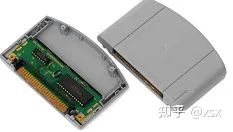
PROM is a programmable ROM that is blank when shipped; users can write information as needed, but once written, it cannot be changed. PROM achieves 0/1 writing by melting fuses inside with a voltage of 20V. Thus, PROM is one-time programmable; once the fuse is melted, it cannot be restored. To write new data, a new PROM is required. A typical example of PROM is the Nintendo game cartridge.
Programmable ROM is blank when shipped, allowing users to write information as needed, but once written, it cannot be changed. PROM achieves 0/1 writing by melting internal fuses with a voltage of 20V. Thus, PROM is one-time programmable; once the fuse is melted, it cannot be restored. The high programming voltage of PROM and its one-time programming nature are not suitable for long-term development.
EPROM (Erasable Programmable Read-Only Memory)
EPROM is a programmable and erasable memory. The working principle of EPROM involves high voltage conditions for programming and ultraviolet light exposure to erase the chip’s contents. This method allows for high-voltage programming and ultraviolet erasure, making it reusable. However, the cost is high and it is not widely adopted.
EEPROM (Electrically Erasable Programmable Read-Only Memory)
EEPROM is electrically erasable and programmable, allowing for erasure and programming at conventional voltages. It can be programmed and erased under 3.3V-5V conditions, supporting multiple programming and erasure cycles.
Flash Memory

Flash memory allows for block erasure and writing, with advantages such as lightweight, low power consumption, and small size. However, it requires prior identification before writing, and block erasure is limited, leading to read/write interference. Common examples include USB drives and SD cards. In the block diagram, if a user downloads the binary program code to an external USB drive, the CPU can boot from the USB device by controlling the USB interface during power-up. This means that the first instruction executed by the CPU is initiated from the file on the USB. However, during the writing process, it is crucial to ensure that the data on the USB is clean and only contains the program required by the CPU.
During the process of reinstalling the operating system on a PC, the first step is to store the Windows system on a clean USB drive, then write the operating system data to the hard drive. After powering on the computer, it runs the operating system data from the hard drive, which means that the USB and hard drive both belong to flash memory.
Returning to the initial question, how can data be read and written in everyday life if ROM cannot store it? For instance, how does STM32 store data? ROM serves as program storage; data does not change after power loss, but during program execution, its data remains unchanged. Early microcontroller ROMs, due to the cumbersome process of erasing and rewriting, or the low-cost OTP type that cannot modify data, have been replaced by modern flash memory.
Due to the ease of erasing and writing in flash memory, some modern microcontrollers support online programming, enabling specific program execution modes to modify the content of flash memory, allowing for online changes to program storage. This does not conflict with the notion that the contents of program storage cannot be altered during normal operation since it operates in read-only mode.
RAM (Random Access Memory)
RAM is the internal storage that exchanges data directly with the CPU. It can be read and written at any time and is fast, typically serving as temporary storage for the operating system or other running programs. RAM can be further divided into Static Random Access Memory (SRAM) and Dynamic Random Access Memory (DRAM). SRAM has the advantage of fast access but is more expensive to produce; a typical application is caching. DRAM is widely adopted as the main memory due to its lower unit capacity price.
Characteristics of DRAM:
-
• Random Access: Random access means the time required to read or write messages in memory is independent of the location of that information. In contrast, serial access memory includes sequential access memory (like tapes) and direct access memory (like disks).
-
• Volatile: RAM cannot retain data when the power is turned off. To save data, it must be written to a long-term storage device (like a hard drive). The main difference between RAM and ROM is that data stored in RAM is lost after power loss, while ROM retains its data.
-
• High Access Speed: Modern random access memory is among the fastest writing and reading devices available, with access latency being negligible compared to other mechanical storage devices (like hard drives and optical drives). However, it is still slower than SRAM, which is used as CPU cache.
-
• Requires Refreshing: Modern RAM relies on capacitors to store data. When a capacitor is charged, it represents 1 (binary), while an uncharged capacitor represents 0. Due to leakage, the charge may gradually dissipate over time, leading to data errors. Refreshing refers to recharging the capacitors to compensate for lost charge. DRAM’s reading also has a refreshing effect, but general timed refreshing does not require complete reads; it only needs to select a row (Row) within the chip to refresh all data in that row simultaneously.
-
• Sensitive to Static Electricity: Like other fine integrated circuits, RAM is very sensitive to static electricity. Static can disrupt the charge in the capacitors, leading to data loss or even damaging the circuit. Therefore, one should touch a metal ground before handling RAM.
SRAM
Static Random Access Memory (SRAM) is a type of random access memory. The term “static” means that this memory can maintain the stored data as long as power is supplied. In contrast, data in Dynamic Random Access Memory (DRAM) needs periodic updating. However, when power is cut off, data stored in SRAM is also lost (it is classified as volatile memory), which is different from ROM or flash memory that can retain data after power loss. SRAM is more expensive than DRAM but is faster and has very low power consumption (especially in idle states). Thus, SRAM is preferred for applications requiring high bandwidth or low power consumption, or both.
SRAM is easier to control than DRAM and is also randomly accessible. Due to its complex internal structure, SRAM occupies more area than DRAM, making it unsuitable for applications requiring higher storage density at lower costs, such as PC memory.

As mentioned earlier, when the CPU is powered on, the first instruction is obtained from ROM. The process is shown in the red line of the diagram. The disk contains the initialization of the operating system (if it is pure bare metal, it includes the interrupt vector table and some initialization values). Once the CPU receives instructions, it writes these initialization data to RAM (as shown in the yellow line of the diagram), and then reads data from RAM (as shown in the green line of the diagram) to execute instructions. The process is illustrated in the diagram.
From the above, we can see a question: why does the CPU write data from ROM to RAM before reading it? Isn’t it faster to read data directly from ROM?

For example, if you have a 1TB video on your computer’s mechanical hard drive that you want to share with a friend, there are two options: the first is to take your computer and drive for an hour to your friend’s house, copying the video to their computer, which takes two hours total (one hour driving, one hour copying). The second is to send your friend a link to download the video from a cloud storage service, which might take 11 days to complete, but your friend can start watching the video while it downloads.
Although the time taken for direct data transfer from ROM to CPU is indeed longer than the time taken for the process ROM -> CPU -> RAM -> CPU, the speed of data retrieval from RAM is far faster than from ROM. Given that data transfer from ROM to CPU consumes significant time, is there a way to directly write data from ROM to RAM?

Modern computers use DMA technology to avoid the time loss from ROM to CPU, as shown in the red line of the diagram. Additionally, a cache can be added between ROM and CPU to store some data, speeding up the CPU’s reading of programs. This cache is also known as a “solid-state drive”.
In the above process, we clarified the general process of CPU data retrieval. At the moment the CPU is powered on, ROM holds our program data and operating system. After the CPU reads data from ROM, it writes it to RAM, and then reads it from RAM. When the user presses the save button, the CPU reads from RAM and writes the data back to ROM (here, ROM refers to flash memory, which is read/write capable). With this foundation, we can delve deeper into the three main processes of the CPU and the role of the PC (Program Counter).
When discussing memory, the concept of the stack is often mentioned. So what is a stack? What is its purpose?
Stack
A stack, also known as a stack or stack structure, is a type of data structure where data items are arranged in order, allowing insertion and deletion only at one end (the top of the stack).
In microcontroller applications, the stack is a special storage area primarily used to temporarily store data and addresses, typically employed to protect breakpoints and contexts. The size is defined by the programmer. When programmers mention “putting data in the stack”, they usually refer to the “stack area” (as this is where data is stored).
In simple terms, the purpose of the stack is to better allocate memory (RAM and ROM). Since each piece of data stored in memory has a corresponding address, C language has a special type of data called pointers, which generally point to the address where the data is stored.
Think of memory as a series of small black rooms containing data, where each room has a lock (address). A pointer is a key; the user can release data from the room using the pointer (the address the pointer points to allows access to the data within the room). The capacity of memory is vast (the number of small black rooms is large), so it is essential to manage memory effectively, and stack management is undoubtedly the best method.
From the above, we understand that the PC register loads instructions from the instruction register one by one, but in C language, programs do not run sequentially. Sometimes, a function may jump to another function. How should the address of the original function be saved?
Method one: Using an internal CPU register.
A special register can be added to the CPU to store the address of the original function (this register is temporarily referred to as the “address register”). After the sub-function runs, the PC register can be directed back to the address register, completing the function jump. However, if multiple sub-functions are nested within each other, using N address registers would be impractical. Clearly, using address registers only works for a small number of function jumps, so what should be done for deeply nested functions?
Method two: Use the stack to store addresses during function nesting.
To better understand this process, one needs to have a basic understanding of stacks.
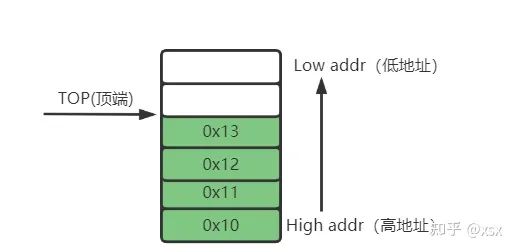
As shown in the diagram, memory is a continuous address storage space, so the stack is also a continuous storage space. Additionally, the stack stores a large amount of data for CPU use. When the CPU needs data from the stack, it retrieves it, and the results of CPU operations must also be stored in the stack. This “retrieval” and “storage” process will inevitably change the number of data items. Thus, it is necessary to establish a mechanism to determine how much data is currently in the stack; this is where the stack pointer register (SP) comes in. Its function is illustrated in the diagram:

We know that the stack is a section of storage space in memory. As shown in the diagram, the stack has a high address at the bottom and a low address at the top. The stack functions like a storage jar that is sealed on one side and open on the other. The SP is a pointer register that points to the current address of the stack. In the diagram, when data 1111111 has not yet been stored in the stack, the stack is empty, and the current SP points to the bottom.
When the CPU writes data into the stack (the data 1111111), the SP decreases (to 11111, freeing up a space), and the SP points to the address of 1111111; this process is called “pushing” onto the stack. Similarly, when 2222222 is pushed onto the stack, the SP pointer points to the address of 222222. When popping 111111, the SP address must first increment (to reclaim the data space) and then pop the data of 2222222, and finally increment the SP to pop 111111. This demonstrates the first-in, last-out concept of the stack.
From the above analysis, we can summarize the following characteristics of the stack:
-
• The stack is a continuous storage space.
-
• The stack operates on a last-in, first-out basis.
-
• Data can only be added or removed from the top of the stack.
-
• The stack maintains the order of data.
There are two basic operations for the stack:
-
• PUSH: Adds content to the top of the stack.
-
• PULL: Retrieves content from the top of the stack.
Why are the characteristics and operational methods of the stack defined as such? The PC is the program counter within the CPU, which always points to the address of the next instruction. The PC determines the order in which the instruction register (IR) retrieves instructions, and IR executes instructions one by one in sequence (unless a jump instruction occurs).
The stack operates on a last-in, first-out basis. Earlier, we raised the question of how to protect the context when a function is called. Using internal CPU registers to save the address can solve the issue, but for multiple nested functions, using the stack to store the jump addresses provides a more effective solution.
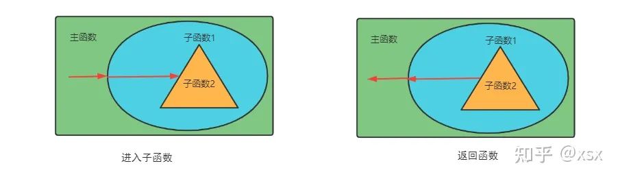
To better understand this process, we can analyze the concept diagram.

As illustrated, when the main function calls sub-function 1, and sub-function 1 calls sub-function 2, the operational process is as follows: the main function encounters a call to sub-function 1, jumps to execute it, and while executing sub-function 1, it encounters a call to sub-function 2. Thus, sub-function 2 runs and, upon completion, must return to the main function (where there are still unfinished tasks).

When the main function calls the sub-function, it pushes the current address of the main function onto the stack, then jumps to execute sub-function 1. When sub-function 1 calls sub-function 2, it also pushes the current address onto the stack. After sub-function 2 completes execution, it pops the previously saved address from the stack, allowing the CPU to return to sub-function 1 and continue executing the main function.
From the above, we can conclude that the stack can also be used to pass parameters and return values (in C language, this is known as pre-press function calls).
Assembly programs can use the stack to save local variables and register values.
CPU hardware uses the stack to save return addresses and register contexts (during interrupts).
The stack’s top position is determined by the stack pointer register (SP) within the CPU.
The initial position of the stack is set by the program code, pointing to the predefined bottom of the stack space.
If you want to manipulate the stack yourself, remember: whatever you put in the stack, you must retrieve.
In the above example, we can summarize the process of CPU and stack interaction to better encapsulate the knowledge points discussed.
#include<stdio.h>

void SubFunc()
{

}
int main()
{
  int A=1;
  int B=2;
  int C;
  SubFunc();
  C=A;
  A=B;
  B=C;
  return 0;
}
The code for swapping the values of A and B is compiled into assembly as shown in the figure. Of course, the stack does not store assembly instructions, but rather machine code; for convenience, assembly instructions are displayed within the stack. Initially, there are no instructions running, so the PC points to NOP (no operation).


-
• First: The PC points to the next instruction’s address (SubFunc), and the SP decreases, pushing the values of A and B from the internal general registers onto the stack, as shown in the second diagram.
-
• Second: The PC points to the start address of the SubFunc function, and the SP continues to decrease, pushing the address of PULLA onto the stack for later return use, as shown in the third diagram.
-
• Third: The PC continues to point to the return instruction address within the function; since the sub-function is empty, the SP address does not change, as shown in the fourth diagram.
-
• Fourth: The PC points to the PULLA instruction address; after the CPU receives the RTS instruction, the SP increments, popping the previously saved address from the stack. As shown in the fifth diagram.
-
• Fifth: The PC continues to point to PULLB, and the SP increments, popping the value 22 from the stack and overwriting the internal register for A. This achieves the assignment of B’s value to A.
-
• Sixth: The PC continues to point to the next instruction’s address; the SP increments, popping A’s value and overwriting the internal register for B. This achieves the assignment of A’s value to B.
Through the above steps, the values of A and B are successfully swapped. We can observe that the value of C does not appear in this process, as C is merely defined but has no actual size, allowing the compiler to optimize it away.
In the above example, we can see that both instructions and programs are stored in the stack. How should the instruction data be managed? There are generally two management structures: the Von Neumann architecture and the Harvard architecture.
Von Neumann Architecture and Harvard Architecture
Von Neumann Architecture
Early computers were composed of various logic gates, assembled into a fixed circuit board to execute a specific program. If a program’s functionality needed to be modified, the circuit board had to be reassembled, making early computer programs hardware-based! In early computers, programs and data were two distinct concepts: data was stored in memory, while the program was part of the controller.
This inefficient computing process led to Von Neumann’s proposal to encode programs and store both data and encoded programs in memory, allowing the computer to call the program stored in memory to process data. This means that any program ultimately converts to a binary format stored in memory, and to execute the corresponding program, the computer only needs to sequentially fetch and execute instructions from memory. The essence of Von Neumann architecture is to reduce hardware connections, leading to the separation of hardware and software, meaning hardware design and program design can be executed separately. The core ideas of Von Neumann architecture are as follows:
-
• Programs and data are ultimately in binary form, and both programs and data are stored in memory in binary form, which is the executable binary file: .bin file.
-
• Programs, data, and instruction sequences must all exist in main (internal) memory to facilitate the computer’s ability to quickly extract and analyze instructions during operation.
-
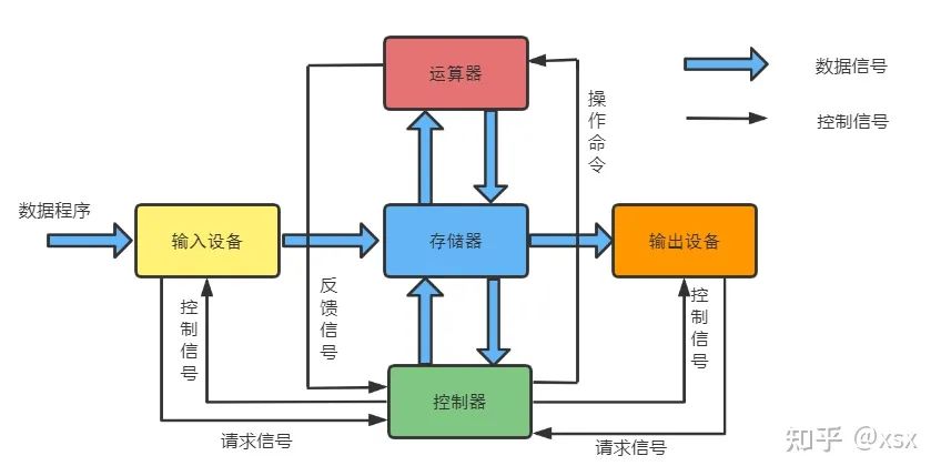
• It defines the five basic components of a computer: the arithmetic unit, control unit, memory, input devices, and output devices.
The following code illustrates the operational process of Von Neumann architecture.


This analysis skips the process of loading ROM data into RAM during startup (as previously discussed, ROM->CPU->RAM) and instead focuses on the general process of fetching instructions from the CPU and RAM, analyzing, and executing them.
-
• First: During the power-on process, the PC obtains the initial instruction and stores it in the address register (MAR).
-
• Second: The MAR retrieves the data from memory at address 0 and stores it in the data register (MDR).
-
• Third: The MDR transfers its value to the instruction register (IR) via the data bus.
-
• Fourth: The IR sends the opcode to the control unit (CU); after analysis, it determines that this is a data-fetching instruction and calls the MAR to retrieve the data.
-
• Fifth: The MAR retrieves data from memory and places it in the MDR, which is then placed in the accumulator (ACC) under the control of the CU.
-
• Sixth: The PC automatically increments, repeating steps 1-4.
-
• Seventh: Since a multiplication operation is executed, the CU places the value of b from the MDR into MQ and the value of a from the ACC into X, directing the ALU to perform the calculation, storing the result in the ACC. If the product is too large, MQ will act as auxiliary storage. This ultimately achieves y=a*b+c.
From the above, it is evident that the data in memory consists of 16 bits, with the first 6 bits as the opcode and the last 10 bits as the address code. The CU decodes the opcode to identify whether it is a read, write, or jump instruction, while the address code identifies the corresponding data in memory for operation. This reinforces the idea of Von Neumann architecture, where data and instructions are stored in the same register.
From the above process, we can also answer the questions raised earlier. The PC register is used to store the address of the next instruction (it can also store the address of the current instruction; however, since registers are temporary, it is more accurate to view it from the perspective of the next step).
Harvard Architecture
The Von Neumann architecture is widely used in today’s computers. However, we cannot assume that all computer architectures are the same. In modern society, high-performance microprocessors such as 89C51, STM32, and ARM differ significantly from traditional computers in two main ways.

In computers, RAM corresponds to computer memory modules, while ROM corresponds to computer disks. Computer RAM typically exceeds 8GB, and disks usually exceed 500GB. In contrast, microprocessors have RAM and ROM capacities that rarely exceed KB, with ARM’s RAM ranging from hundreds of MB to 1GB, and ROM in the GB range. Microprocessors integrate ROM, RAM, SPI, ADC, USB, NVIC, and other drivers, forming a CPU+ model.
Secondly, during instruction execution, data and instructions are not stored in the same memory. Instructions are stored in instruction memory, while data is stored in data memory.
The separation of instruction and data storage, where they do not interfere with each other, is the main feature of the Harvard architecture.

As shown in the diagram, this is a typical Harvard architecture. Instructions and data are stored separately. Compared to Von Neumann architecture, Harvard architecture does not require decoding before operating data, allowing for simultaneous use of instructions and data, which significantly enhances operational efficiency.
Clock
Why does the CPU need a clock?
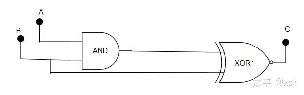
First, let’s analyze the logic circuit in the diagram: when A=B=1, C=0. When the input signal changes, the logic element does not immediately respond to the input change; there is a propagation delay. When B changes to 0, the XOR gate detects the input change and outputs 1, but due to propagation delay, the output of the AND gate takes a little longer to change to 0, leading to an unstable output state.
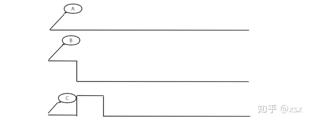
This phenomenon is called a race condition, where an unwanted pulse signal appears in the output. A simple solution is to place a clock edge-triggered flip-flop at the output.
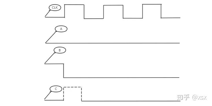
The edge-triggered flip-flop ensures that the output only responds to changes in the D input when the CLK input transitions from 0 to 1. This hides all propagation delays, stabilizing the output state.
From the above example, we see why the CPU needs a clock: most microprocessors are driven by synchronous timing circuits, which consist of various logic gates. Logic gates require a small amount of time to respond to input changes (propagation delay), so clock cycles must accommodate these delays, and the clock cycle should be long enough to accommodate all logic gate propagation delays.
Of course, there are also asynchronous sequential logic circuits that do not require clock signals for synchronization. However, while these asynchronous logic circuits are faster than synchronous ones, they are much more complex to design and are prone to race conditions. Therefore, most CPUs still require clocks for signal synchronization.
This section primarily discussed the CPU operation process. The next section will delve into concepts such as ARM interrupts and buses, laying the foundation for a better understanding of RTOS.
Copyright Statement: This article is sourced from the internet, freely sharing knowledge, and copyright belongs to the original author. If there are any copyright issues, please contact me for deletion.