Author | Lin Nova
Produced by | Automotive Electronics and Software
This article mainly introduces the principles of embedded kernel architecture and the current mainstream MCU kernel architectures in the embedded market.
#01
1.1 Introduction to Kernels
Computer chip kernel architecture refers to the basic design and organizational structure that makes up a microprocessor chip. It defines how the processor executes instructions, processes data, and controls program execution. Simply put, if the brain is likened to the CPU, the kernel architecture is analogous to the composition and working principles of various centers within the brain. Different series of chips adopt different kernel architectures based on usage scenarios and requirements.
The computer kernel is inseparable from the kernel instruction set, which is a specific form of the programming interface of the computer kernel. It organizes the operations of the computer kernel into a set of instructions that can achieve kernel control through integration and decomposition.
Different kernels have different kernel instruction sets. For example, the computers we commonly use (Intel or AMD chips) use the X86 instruction set, and the kernel belongs to the X86 architecture. Other common architectures include ARM, DSP, and RISC-V. When we want to master a specific chip and build a system based on it, we must understand the kernel of that chip.
The relationship between the kernel and the instruction set is close and complex. Each kernel architecture has a corresponding instruction set, and there is a version matching relationship between the kernel and the instruction set. For example, the Cortex-A8 and Cortex-A9 kernels are based on the ARMv7-A instruction set architecture, while the Cortex-M3 and Cortex-M4 are based on the ARMv7-M instruction set architecture. Here, “v7-A” and “v7-M” refer to the versions of the instruction set architecture, representing the types of instruction sets they support.
1.2 Classification of Kernels
Computer kernel instruction sets can be divided into two types based on instruction types. One is the Reduced Instruction Set Computing (RISC), which is a computer processor architecture design philosophy that aims to keep the instruction set relatively small and simple to improve execution efficiency. RISC architecture emphasizes completing operations with fewer and more fundamental instructions, and these instructions have relatively short execution times.
The other type is the Complex Instruction Set Computing (CISC), which is a computer processor design model characterized by supporting a large number of complex instruction systems. The design philosophy of CISC architecture is to use some complex instructions to implement commonly used functions that were originally implemented by software, thereby improving the execution speed of the computer. This design allows CISC architecture processors to have a wide variety of instructions, including basic arithmetic logic operations, data transfers, control transfers, processor state management, advanced data processing, and system-level instructions.
The classification of kernels generally matches the instruction set, as they are co-evolved designs. For example, the kernel architecture that pairs with the reduced instruction set is the reduced instruction set kernel architecture.
Chips in the embedded field generally adopt reduced instruction set kernel architectures, which align with the characteristics of low resource demand and high real-time requirements in the embedded field.
#02
From the perspective of computer principles, kernel architecture mainly includes the kernel’s computation methods, instruction systems, CPU structure and functions, interrupt systems, etc.
2.1 Kernel Data Types and Computation Methods
Each kernel has its fixed data types involved in computation and their arithmetic operations within the kernel.
For data types, the kernel’s data types can be divided into two types: signed and unsigned. They are implemented in memory in the form of original code, complement code, and reverse code.
|
|
|
|
|
|
|
|
|
|
|
|
|
|
|
|
|
|
|
|
|
|
|
|
|
|
|
|
|
|
|
|
|
|
|
|
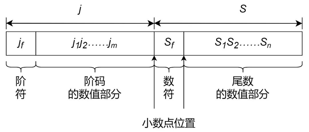
For the representation of decimals, they are divided into fixed-point and floating-point numbers. Fixed-point numbers have the decimal point in a fixed position, while floating-point numbers use scientific notation to divide values into four parts. Embedded kernels generally use floating-point representation.
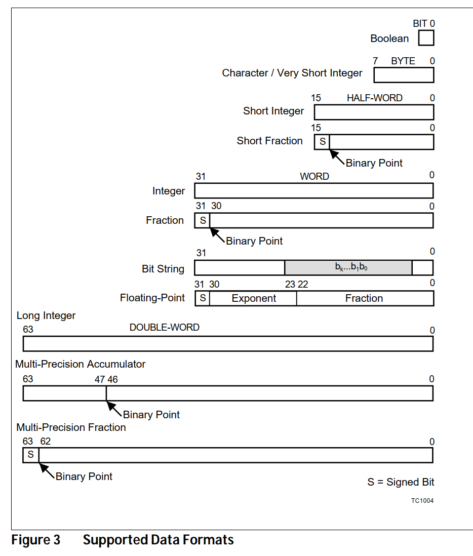
Generally, these data types are supported across various embedded systems without significant differences. The following image shows the data types supported in the Infineon TriCore 1.6.2 architecture.
In terms of computation methods, the RISC architecture mainly includes addition, subtraction, multiplication, division, shifting, etc. Different kernel hardware processing methods may exhibit slight differences in speed.
2.2 Instruction System
As we know, when writing embedded code, we use high-level languages such as C; then we need to use a compiler to compile it into machine language, which is assembly language; ultimately, it is burned into the machine, and the kernel decodes it to execute it.

For ordinary programmers, they only need to learn high-level languages like C or C++, and generally do not need to care about lower-level details, as the compiler will handle the isolation.
For different types of kernel architectures, due to their different internal hardware mechanisms, different machine languages are generated, and corresponding machine languages need to be provided to users. Each machine language statement is commonly referred to as a machine instruction, and the entire set of machine instructions is known as the machine’s instruction system.
Different kernels have distinctly different instruction systems, even among the same series like ArmV7-M and ArmV7-A.
Instruction Format
Instructions generally consist of two parts: operation code and address code.

The operation code indicates the operation to be performed by the instruction, such as addition, subtraction, transfer, shifting, etc. The number of bits reflects the number of operation types the kernel can support. For example, if the operation code occupies 7 bits, the kernel can contain a maximum of 2^7 = 128 instructions.
The address code indicates the address of the source operand, the address of the result, and the address of the next instruction. The address can be a memory address, a register address, or a stack address.
Different kernels have different instruction word lengths. Generally, the instruction word length of embedded MCUs is 32 bits, and most kernels also support 16-bit instructions to reduce code size.
Operands
A complete assembly code generally includes instructions and operands. Common types of operands include addresses, numbers, characters, logical numbers, etc.
The following is the format of an addition instruction in ArmV7-M, which includes two registers and an immediate number:

Addressing Methods
Addressing methods refer to the methods used to determine the data address of the current instruction and the address of the next instruction to be executed. They are closely related to the hardware structure and directly affect instruction format and functionality. Addressing methods can be divided into instruction addressing and data addressing.
Instruction addressing is relatively straightforward, as we commonly see the program automatically incrementing the PC after execution to execute the next instruction, known as sequential addressing. There are also some jump-type instructions, such as Jump, which are known as jump addressing.
Data addressing methods are much more diverse, including immediate addressing, direct addressing, implied addressing, indirect addressing, register addressing, register indirect addressing, base addressing, indexed addressing, relative addressing, and stack addressing.
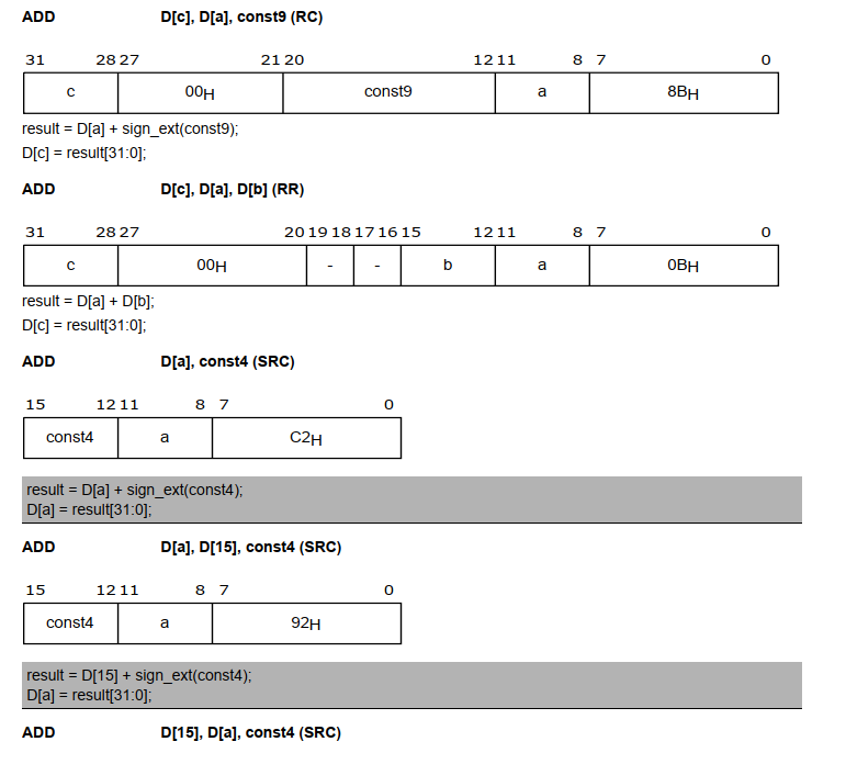
The following image lists several forms of the addition instruction in Infineon TriCore, including immediate addressing, register addressing, implied addressing, etc.
In addition to these conventional data operation instructions, there are also some special instructions with kernel-specific characteristics based on different kernel mechanisms and features, such as the data barrier instruction DSB in ARM and the low context save instruction SVLCX in TriCore.
RISC VS CISC
The RISC instruction system, compared to the CISC instruction system, saves more area in the chip circuit design due to the use of fewer instructions. This area can be used for other functionalities, such as providing more registers.
Additionally, due to the fewer types of instructions, more general-purpose registers, and pipeline design friendliness, RISC generally has a higher operation speed than CISC.
2.3 CPU Structure and Functionality
CPU Structure
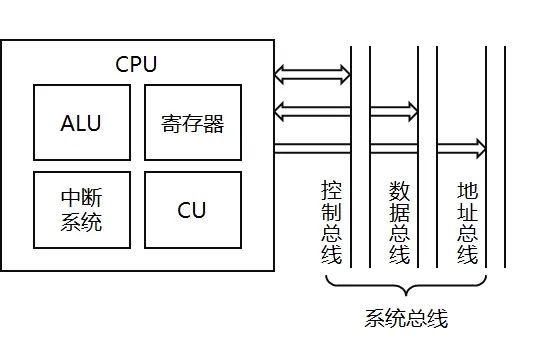
The CPU essentially consists of two major parts: the arithmetic unit and the control unit. As shown in the following image, the minimum system of a general computer kernel includes the logical arithmetic unit ALU, registers, interrupt system, and control unit CU.
Registers
Registers are the fastest, smallest, and most expensive memory in computer chips. They are located within the CPU and are used for various controls and computations. Registers can be roughly divided into two categories: one is ordinary user registers used for regular computations, including general-purpose registers, data registers, address registers, etc.; the other is control and status registers used to control the CPU’s status, generally used by operating systems and other privileged programs.
When we say a chip is of a certain bit, such as 32 bits, it refers to the data processing width of the chip, which is usually also the width of the registers. In the embedded field, the register width of chips is generally 32 bits.
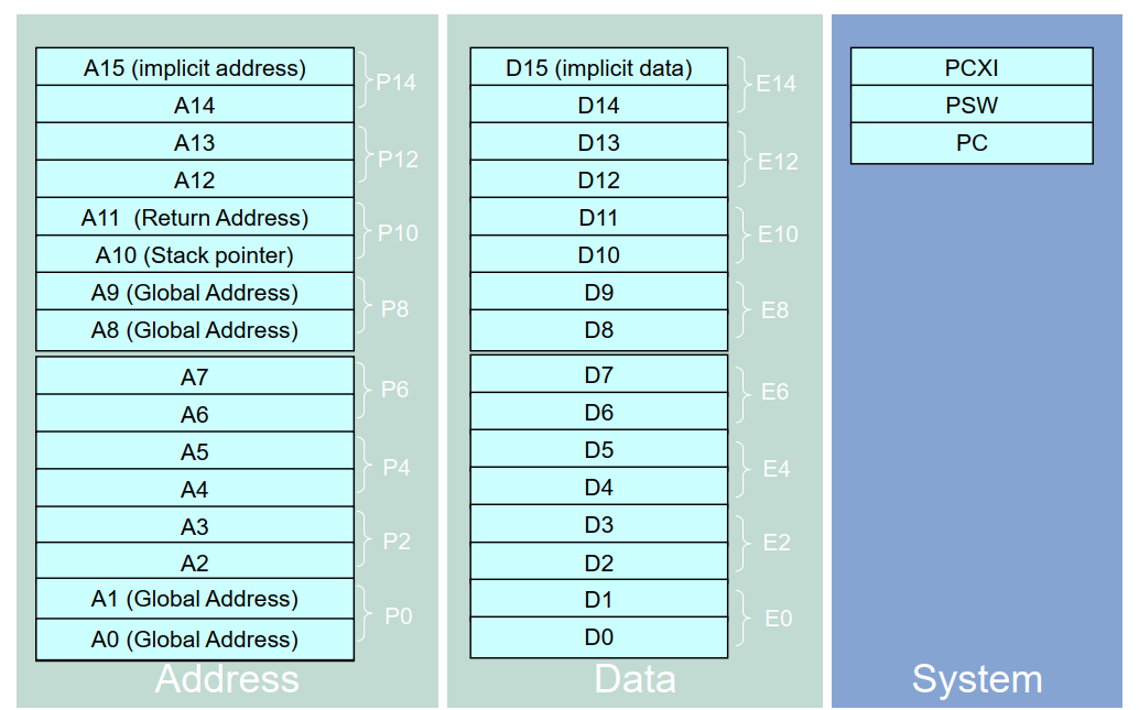
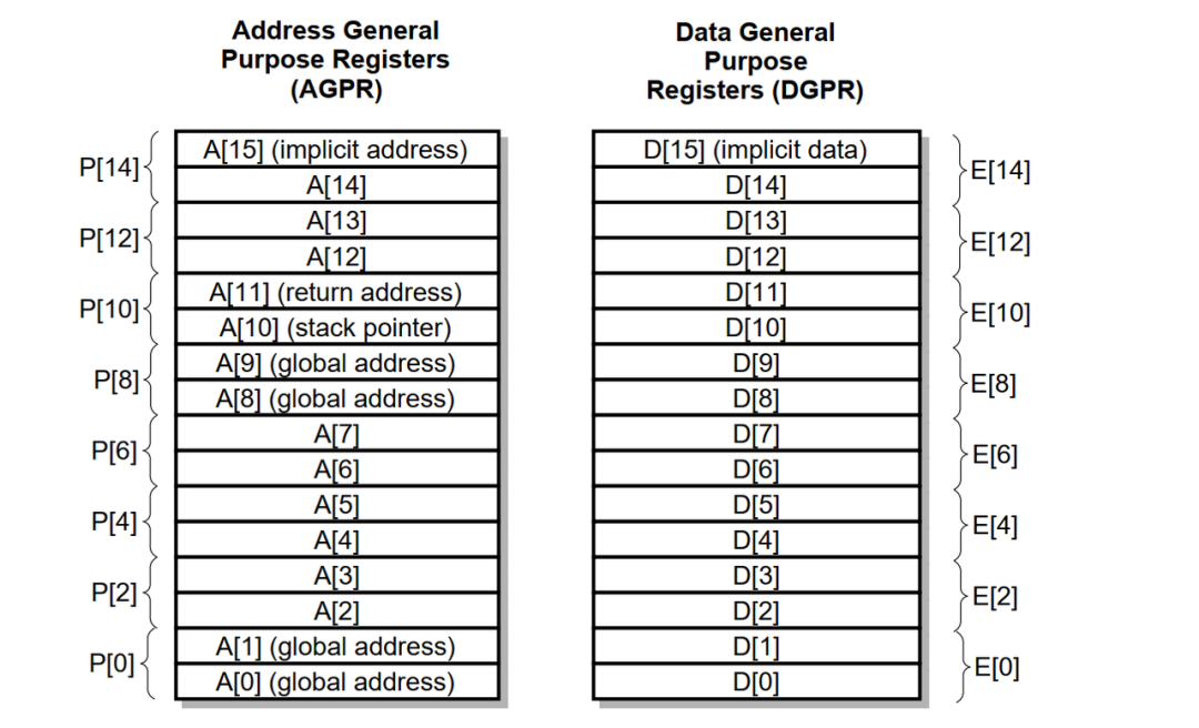
Different kernels have different register structures based on their structural designs. For instance, the following image shows the Infineon TriCore kernel registers, which include 16 regular data registers and 16 address registers, including stack pointer registers and return address registers. The system registers include special registers used for context management.
Instruction Cycle and Instruction Pipeline
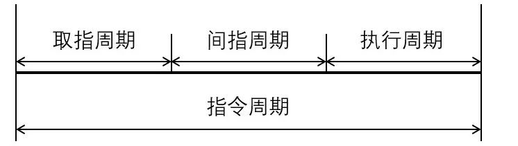
The total time required for the CPU to fetch and execute an instruction is referred to as the instruction cycle. Generally, an instruction cycle includes multiple operational processes. For example, when encountering an indirect addressing instruction, it needs to go through indirect addressing, thus the instruction execution is divided into three parts.
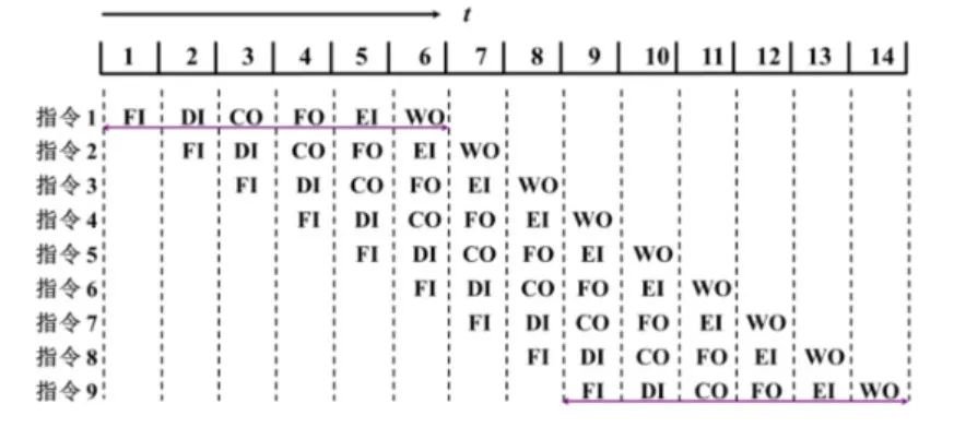
Each operation process of machine instructions in the CPU generally corresponds to a hardware unit, referred to as the instruction unit. These hardware units work in a relay fashion to execute instructions, similar to a pipeline. Assuming we divide the instruction process into six steps: fetch (FI), instruction decode (DI), compute operand address (CO), fetch operand (FO), execute instruction (EI), write operand (WO). As shown in the following image, when the time reaches the second column, instruction 1 has completed FI and entered DI. At this time, the FI instruction unit can fetch the next instruction, achieving parallelism. At the same time, up to six instructions can be processed concurrently (the same column in the image). This technology is known as instruction pipelining, and based on the number of pipeline units, the pipeline in the image is referred to as six-stage pipelining.
Of course, the execution of programs has dependencies, and how smoothly instruction pipelining can be achieved depends not only on the design capabilities of the chip manufacturers but also on the logic of the code. Typically, factors affecting pipelining include structural dependencies, data dependencies, and control dependencies.
Pipelining Superscalar
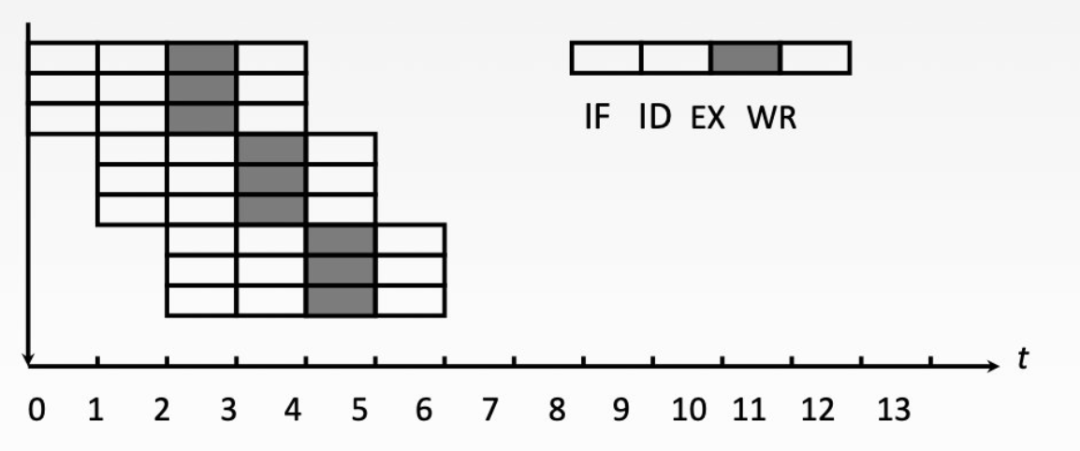
To a certain extent, pipelining technology accelerates program execution spatially. To further develop this, pipelining superscalar technology can produce results for more instructions in a single clock cycle. In simple terms, it means adding multiple pipelines. The most common examples are superscalar technology, super pipelining technology, and very long instruction word technology.
The image below demonstrates the superscalar technology with multiple pipelines running in parallel, showing four levels of three pipelines executing concurrently, with a maximum of 12 instructions executing simultaneously. However, it is also limited by the logic and order of program execution, making it highly dependent on compilation optimization.
2.4 Interrupt System
Whether in the embedded field or other computers, during program execution, interaction with the outside world occurs through I/O, thus receiving various signals from the outside, as well as timer events, program exceptions, and other special events. Timely responses are required for these special events, meaning that the current program must pause and immediately go to the specified code to handle the corresponding logic. This process is referred to as interrupts. Broadly speaking, interrupts include both interrupts and exceptions.
Therefore, for various kernel architectures, an interrupt system needs to be designed to handle various interrupt scenarios.
Interrupt Factors
There are many factors that can cause interrupts, such as manually set software interrupts, data overflow, null pointer exceptions, and hardware failure interrupts. Additionally, once the hardware completes its operation or is ready, it will send interrupts, such as ADC interrupts, SPI interrupts, etc.
Interrupt Response
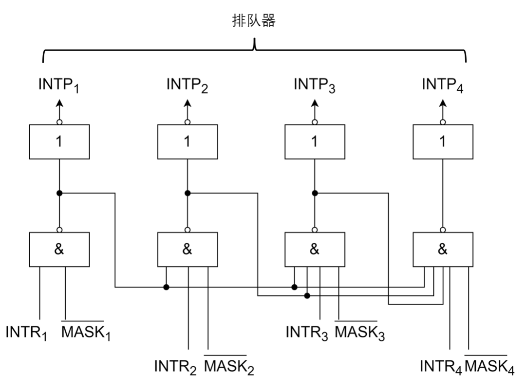
After executing each instruction in the kernel, it will check the interrupt status to determine if any interrupts have occurred. This is also the minimum time granularity for interrupt response. When multiple interrupts occur simultaneously, in the embedded MCU field, they generally need to be prioritized. When a high-priority interrupt is being executed, lower-priority interrupts cannot interrupt it. The image below is a schematic diagram of an interrupt system logic circuit with masking and queuing functionalities.
Interrupt Handling
The interrupt handling process generally includes protecting the scene, processing the interrupt service program, and restoring the scene. Different kernels have different handling mechanisms, and some manufacturers may implement special designs to provide real-time performance, such as the automatic context-saving mechanism in TriCore.
#03
3.1 Current Market Situation of Kernels
The common embedded kernel architectures include the ARM (Advanced RISC Machine) architecture designed by ARM, the RISC-V (Reduced Instruction Set Computer – Fifth Generation) architecture by SiFive, the G4MH architecture by Renesas, and the TriCore architecture by Infineon.
Chip manufacturers generally follow three modes for chip development: one is purchasing kernel licenses for chip design and development, such as buying ARM or Synopsys; another is manufacturers developing kernels on their own; and the third is open-source kernels like RISC-V. The image below lists the current usage of MCU kernels by mainstream manufacturers both domestically and internationally.
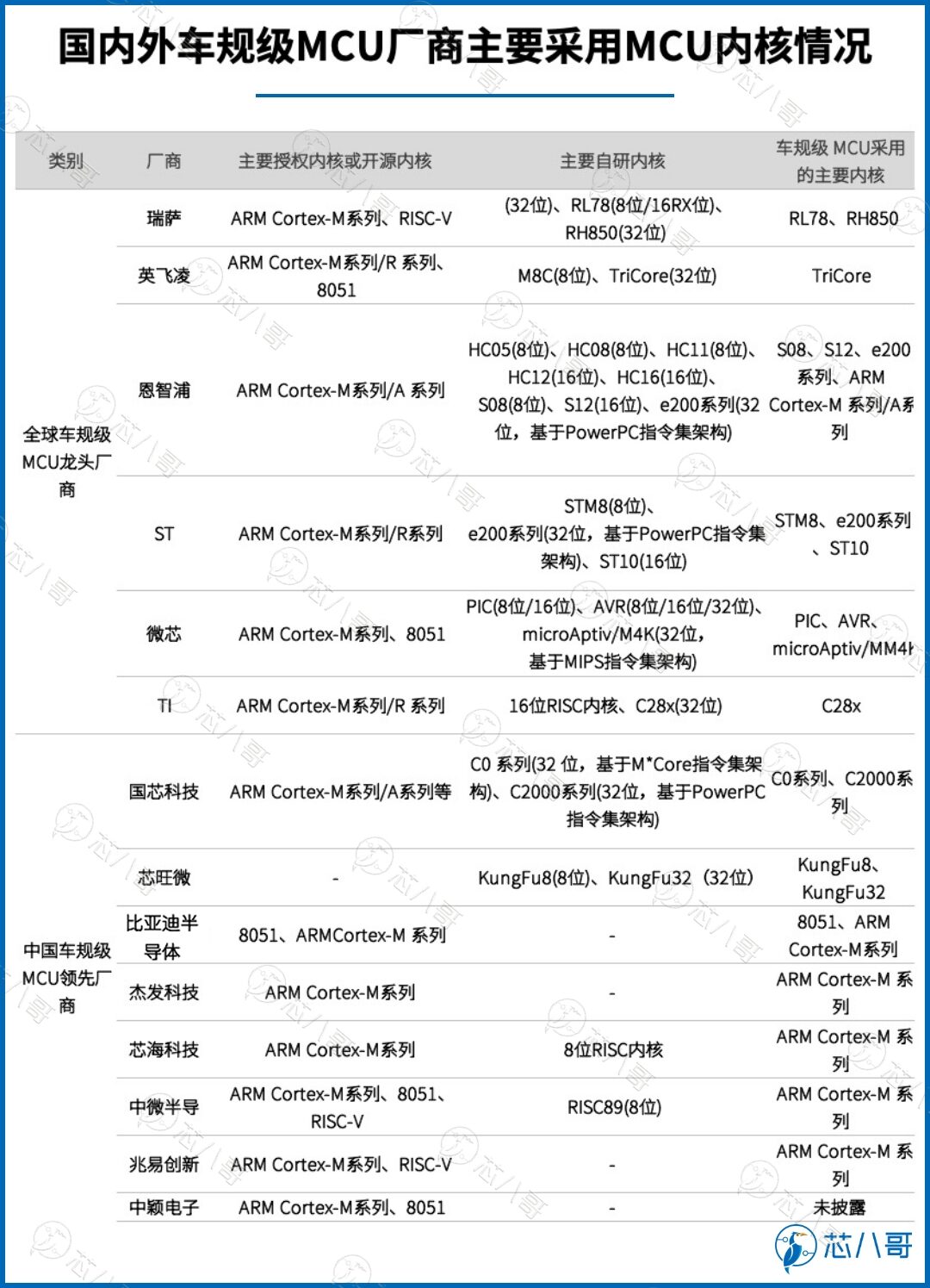
Source: Company financial reports/websites, compiled by Chip Brother
From the image, it can be seen that in the licensing field, major manufacturers generally purchase ARM kernels for their chip development, with the ARM Cortex-M series being widely used in the embedded field. In the open-source field, RISC-V has become the preferred choice for many. After more than a decade of development, it has gradually stabilized. In the self-developed kernel field, the more well-known ones are Infineon’s TriCore architecture and Renesas’ G4MH architecture.
According to statistics, the top three companies in the automotive MCU market, Renesas, NXP, and Infineon, occupy about 70% of the market share.
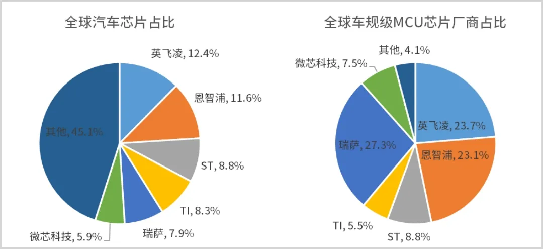
Source: Company financial reports/websites, compiled by Chip Brother
Next, we will introduce three mainstream kernel architectures in the market.
3.2 ARM Cortex-M Kernel
The history of ARM can be traced back to 1978 when Acorn Computers was founded by Chris Curry and Hermann Hauser. In 1993, the Nokia 6110 GSM phone equipped with ARM achieved great success, making the ARM7 processor the flagship mobile design of ARM. Today, over 99% of smartphones worldwide are based on ARM technology.
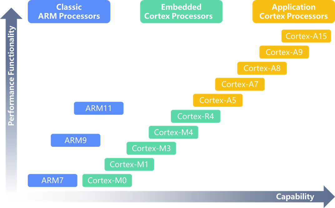
With the company’s development, ARM’s product line has become increasingly diversified, launching Cortex-A, Cortex-R, and Cortex-M CPU processors in the 2000s.
The Cortex series belongs to the ARMv7 architecture (ARM has adopted the Cortex naming convention for products after the classic ARM11). It includes Cortex-A, Cortex-M, Cortex-R, and other products.
Among them:
-
The Cortex-A series is designed for cutting-edge operating systems and user applications based on virtual memory, typically having higher computational capabilities and handling complex computer graphics calculations, mostly used in mobile phones, tablets, and personal computers.
-
The Cortex-R series real-time processors provide high-performance computing solutions for embedded systems that require reliability, high availability, fault tolerance, maintainability, and real-time response, commonly used in autonomous driving, industrial control systems, and medical systems.
-
The Cortex-X series adopts a big core design, significantly enhancing the kernel’s computational capabilities, typically used for servers.
-
The Cortex-M series is specifically designed for microcontrollers, utilizing a reduced instruction set and pipeline structure, with some featuring super pipelining technology, tailored for MCUs with high requirements for real-time performance, power consumption, and safety levels.
The following image shows the performance ladder of mainstream Cortex series products.
In the automotive embedded field, the most commonly used ARM architecture is the Cortex-M series. Since the first Cortex-M processor was released in 2004, the Cortex-M series has developed multiple models, including Cortex-M0, Cortex-M0+, Cortex-M1, Cortex-M3, Cortex-M4, Cortex-M7, Cortex-M23, Cortex-M33, Cortex-M35P, and Cortex-M55, with typical chips being the STM32 series and NXP LPC series.
Cortex-M has the following features:
-
Low Power Design:The Cortex-M series processor cores are designed to be low power, suitable for portable and battery-powered embedded systems.
-
High Performance Processing:Cortex-M processors are characterized by high performance, capable of handling complex real-time tasks with high processing performance.
-
Cost-Effectiveness:Cortex-M processors provide high cost-performance solutions suitable for embedded system designs of various scales.
-
Processor Core:Cortex-M processor cores utilize deep pipelining and a reduced instruction set, aiming to provide high-performance processing capabilities.
-
Interrupt Controller:Cortex-M processors have built-in flexible interrupt controllers that support multiple interrupt priorities and efficient interrupt handling mechanisms.
-
Access Control Unit (ACU):The ACU provides access control to memory and peripherals to ensure system security and stability.
-
Clock and Power Management Unit:Cortex-M processors have rich clock and power management features, providing flexible power management and clock control.
-
Peripheral Interfaces:Support various peripheral interfaces, such as UART, SPI, I2C, etc., for communication with external devices.
-
Instruction Set:Cortex-M series processors support the ARM Thumb instruction set, including 16-bit and 32-bit Thumb-2 instruction sets, as well as optional DSP instructions and floating-point units, providing high-performance signal processing capabilities.
-
Development Support:Designers can choose from many tools available in the ARM ecosystem or use a single, comprehensive toolchain that supports all Cortex-M devices.
-
Architecture Extensions:ARM also provides a series of architecture extensions to meet the needs of next-generation processors, such as DSP extensions, SIMD instructions, floating-point units, and Helium technology, providing additional functionalities and performance for specific application scenarios.
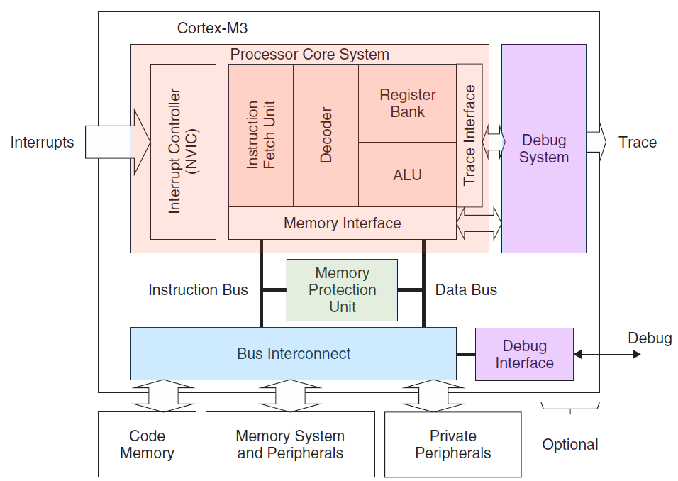
The following image shows the architecture diagram of the Cortex-M3 kernel. From the image, we can see that the Cortex-M kernel includes instruction fetch units, register units, logical arithmetic units, vector interrupt controllers, memory interfaces, etc. It adopts the Harvard architecture with code and data isolation, which is a typical computer kernel architecture.
The instruction set used by the Cortex-M series is the ArmV7-M instruction set, which adopts a typical load-store structure instruction system, utilizing a 32-bit instruction system while also supporting 16-bit thumb instructions. In addition to conventional operation instructions, it supports table lookup jump instructions, conditional execution, hardware division instructions, multiply-accumulate instructions (MAC), and various bit manipulation instructions. The Cortex-M7 features a six-stage dual-issue pipeline, providing higher performance.
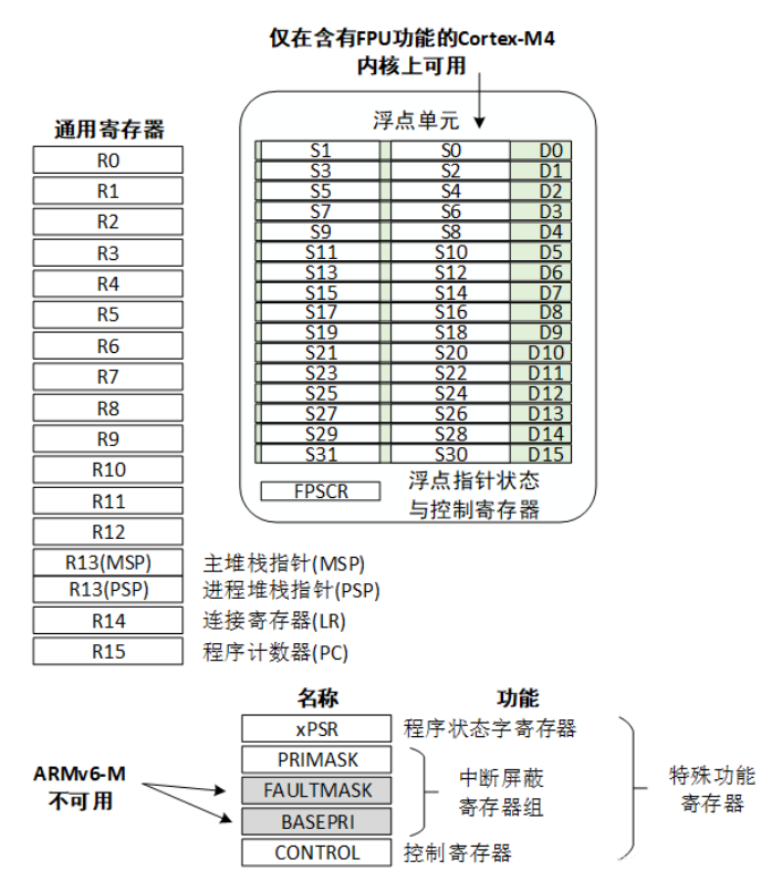
In terms of registers, Cortex-M adopts 16 general-purpose registers and special function registers, including the program status register xPSR and control registers.
In the kernel architecture field, apart from Intel, ARM can be considered the longest-standing manufacturer. Years of development have established its leading position in the industry, making it the preferred choice for licensing kernel IP. Whether in the embedded or mobile field, ARM has a very complete user ecosystem, which is crucial in the chip field as it means lower development and risk costs.
3.3 Infineon TriCore Kernel
In addition to authorized kernels like ARM, some manufacturers also engage in self-developed kernel research, typically strong chip manufacturers like Renesas and Infineon, which are representatives in this field. Here we take Infineon as an example to introduce its TriCore kernel.
Infineon Technologies is a global leader in semiconductor technology, headquartered in Germany, established in 1999 as a spin-off from Siemens’ semiconductor division. As a chip manufacturer with a wide range of technologies, its product line includes power MOSFETs, IGBTs, microcontrollers, sensors, RF chips, etc.
In the microcontroller field, Infineon’s TC2XX and TC3XX series chips are widely known, having a high market share in areas like three electric systems, chassis, and intelligent driving. This includes the TC4XX series, which was just released mid-year, making it a mainstream choice in the automotive industry.
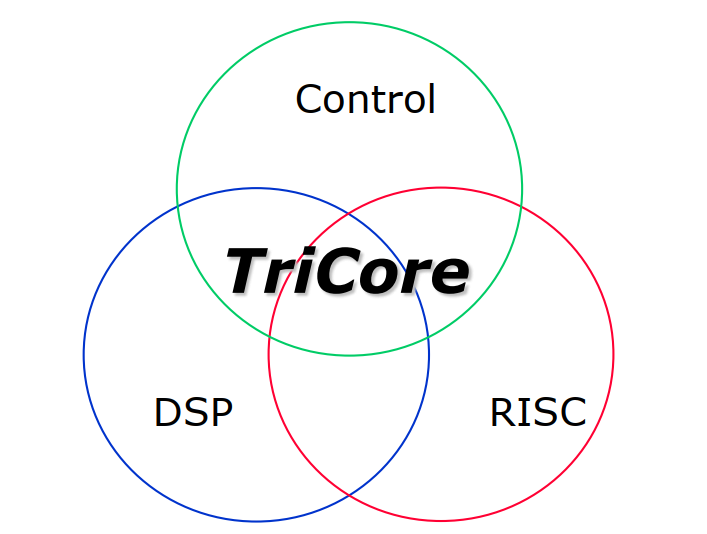
The architecture of the Infineon Aurix2G TC series chips is a hybrid architecture, combining features of both Reduced Instruction Set Computing (RISC) and Complex Instruction Set Computing (CISC), referred to as the TriCore architecture (hereinafter TriCore). It is a 32-bit single-core embedded system architecture optimized for real-time performance (note that this single core does not refer to a single chip core but rather the system architecture involves only one core, with multiple cores operating independently, unlike multi-core architectures). The name TriCore signifies its integration of RISC architecture, DSP architecture, and real-time system technologies, forming a kernel architecture with advantages from all three sides.
The TriCore architecture adopts a high-performance load/store data processing mode of RISC while possessing DSP data processing capabilities. TriCore is a 32-bit computer system, thus adopting a 32-bit address space and supporting optional virtual address space.
Below are the characteristics of the TriCore architecture:
• 32-bit architecture
• 4GB address space
• Simultaneous support for 16-bit and 32-bit instructions, reducing code size
• Most instructions are executed in one cycle
• Branch instructions (using branch prediction)
• Use of parallel data storage to achieve low interrupt latency and fast automatic context switching
• Dedicated interfaces specific to application processors to allow for adding custom instructions
• Zero-overhead loop functionality
• Dual/single clock cycles, 16×16-bit multiply-accumulate unit (optional saturation)
• Optional floating-point unit (FPU) and memory management unit (MMU)
• Extensive bit processing capabilities
• Single Instruction Multiple Data (SIMD) packed data operations (2×16-bit or 4×8-bit operands)
• Flexible interrupt priority schemes
• Byte and bit addressing
• Little-endian byte ordering for data memory and CPU registers
• Memory protection
• Debugging support
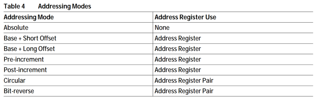
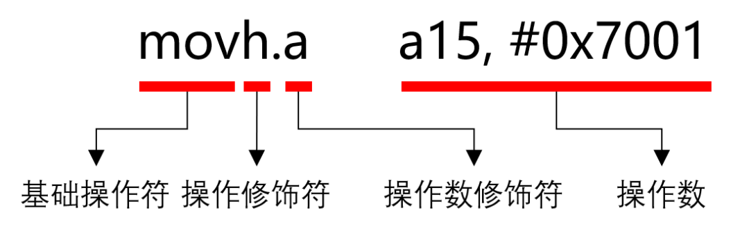
Its kernel uses a 32-bit data format, supporting various basic data types in C language, with address modes adopting little-endian alignment, supporting the following addressing modes.
Compared to ARM kernels, TriCore has two types of general-purpose registers, including 16 32-bit data registers (D[0]~D[15]) and 16 32-bit address registers (A[0]~A[15]), with the separation of data and address registers facilitating efficient parallel execution of arithmetic and memory operations. Additionally, adjacent odd and even registers can be accessed in pairs.
Special function registers include the program counter PC, program status register PSW, previous context register PCXI, and system control register.
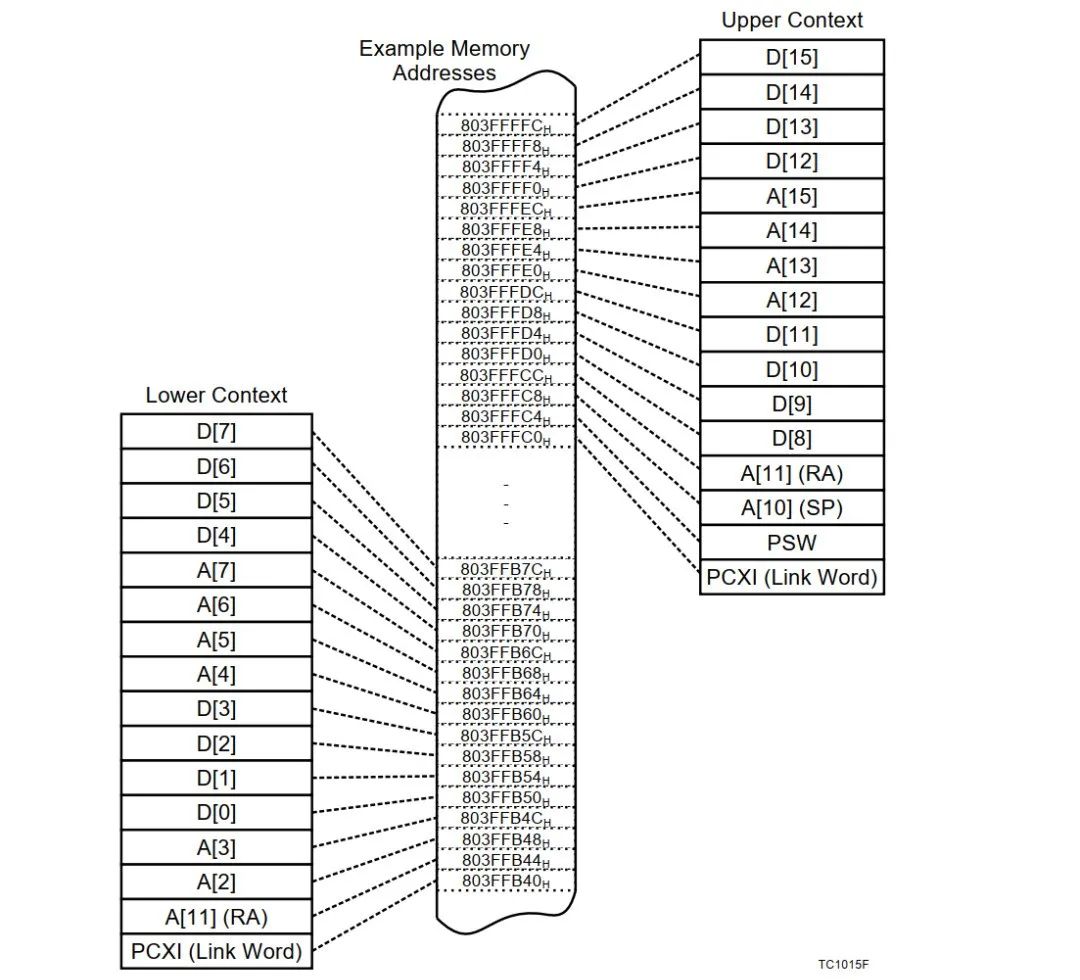
In ARM, the context content is stored in the stack. When a program is called, general-purpose registers and link registers are pushed onto the stack, and upon returning from the call, they are popped from the stack, forming a context-saving mechanism. In contrast, the TriCore kernel has developed a unique hardware context-switching mechanism, where the context is stored in an area called CSA. Although it is also in RAM like the stack, the distinction of management from the stack and the hardware automatic switching mechanism of CSA can effectively improve memory usage efficiency, real-time performance, and security.
The TriCore instruction set also adopts a typical load-store structure, supporting both 32-bit and 16-bit instructions, and supports commonly used microcontroller series processing instructions, as well as some DSP data processing instructions. Compared to ARM, its instruction structure is slightly more complex.
In recent years, Infineon has continued to deepen its focus on the automotive market, continuously innovating and releasing automotive MCU chips that meet current electronic and electrical architecture designs and market demands, holding an irreplaceable position in the automotive MCU field. At the same time, Infineon is also working to expand its user ecosystem, including hosting developer conferences, technical summits, and collaborating with domestic universities, which is also worth learning from domestic chip manufacturers.
3.4 RISC-V Kernel
The last type of kernel is the open-source kernel, with the representative being the widely adopted RISC-V kernel in self-developed chips. Although ARM is convenient for licensing, it faces influences from international political situations and licensing fees. Therefore, a popular technical route for domestic chips is to self-develop based on open-source RISC-V.
RISC-V is an open-source instruction set architecture that originated from a research project at the University of California, Berkeley. RISC-V is the fifth generation of the RISC architecture, with its development history tracing back to 2010, when the research team decided to develop a completely new instruction set after comparing existing instruction sets like ARM, MIPS, SPARC, and x86, finding them complex and entangled with many intellectual property issues.
With technological advancements, RISC-V has found increasing applications in embedded systems, the Internet of Things, and AIOT, with many enterprises and research institutions beginning to adopt RISC-V for product development and research. Its open-source nature provides a platform for global chip designers to innovate without restrictions, indicating that RISC-V will play an increasingly important role in future technological development.
The image below shows a block diagram of a RISC-V processor from SiFive.
RISC-V has the following characteristics:
-
Modular Design:The RISC-V architecture adopts a modular design, allowing users to select suitable modules based on specific needs for customized processor designs.
-
Open Source:The open-source nature of the RISC-V architecture means anyone can view, modify, and distribute the source code, promoting widespread support and development.
-
Flexibility:The RISC-V architecture supports various instruction set extensions, such as vector instructions and floating-point instructions, allowing processors to adapt to different application scenarios.
-
Cost Reduction:The open-source nature allows users to use the RISC-V architecture for free, reducing the development costs of processors.
-
High Performance:RISC-V adopts a reduced instruction set design, characterized by simplicity and efficiency, while the modular design allows for optimizing processor structures to improve performance.
-
Enhanced Security:The RISC-V architecture features robust security characteristics, such as hardware-level isolation, encryption, and tamper-proofing.
The instruction set of RISC-V includes the following types:
-
R type (register-register operations);
-
I type (immediate operations);
-
S type (store operations);
-
B type (branch operations);
-
U type (upper operations);
-
J type (jump operations);
-
C type (compressed operations);
-
F type (floating-point operations);
The instruction format is relatively simple, for example, ADD rd, rs1, rs2 (adding the values of rs1 and rs2, storing the result in rd).
The instruction format design of RISC-V allows it to execute efficiently in modern processors while maintaining enough flexibility to support various computing tasks. This design philosophy is one of the key reasons for RISC-V’s popularity.
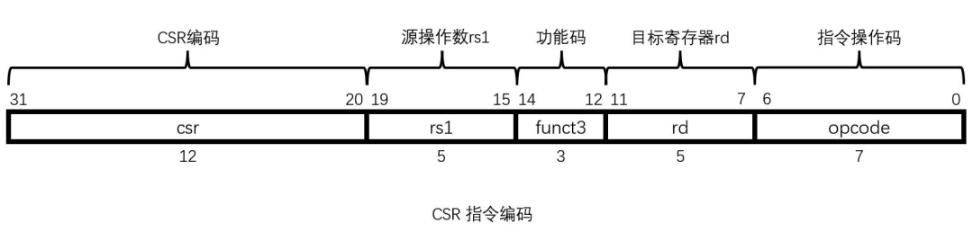
The RISC-V architecture includes 32 general-purpose registers and a series of control and status registers (CSR).
On March 2, 2023, at the Xuantie RISC-V Ecosystem Conference, Academician Ni Guangnan stated that due to the modular, scalable, easy-to-customize, and non-monopolistic advantages of RISC-V, it has become the most popular architecture in the Chinese CPU field.
#04 In today’s embedded field, the mainstream licensed kernels are still the ARM series, which is also the most chosen IP by chip manufacturers both domestically and internationally. Some manufacturers opt for Synopsys automotive MCU kernels. Some manufacturers, such as Infineon and Renesas, have self-developed kernels, and their respective chips occupy a significant market share in the automotive field. Meanwhile, the open-source kernel architecture RISC-V is emerging as a strong contender, favored by manufacturers with self-development layouts both domestically and internationally. Embedded Technology Exchange Group DIY Activities in the Breadboard Community are Ongoing!👇 https://mbb.eet-china.com/forum/topic/147007_1_1.html Share your DIY electronic designs in the Breadboard Community Blog/Forum, and add the tag [Electronic DIY] when publishing the article. There is no word limit, and articles will be reviewed by the community, with rich rewards for you! 【Award Settings】 【Article Requirements】 1. Content must beoriginal and must be related to the electronics industry, and first published on the internet. 2. Content should include: design ideas, finished product display (such as circuit diagrams, functionality display, cost control plans or lists, code, etc.), core intellectual property content may not be displayed. 3. During the event, the same ID can participate multiple times; under the same quality conditions, multiple submissions can accumulate scores. Event Time: November 13, 2024 – February 13, 2025 


 Click to read the original text to learn about the event details!