
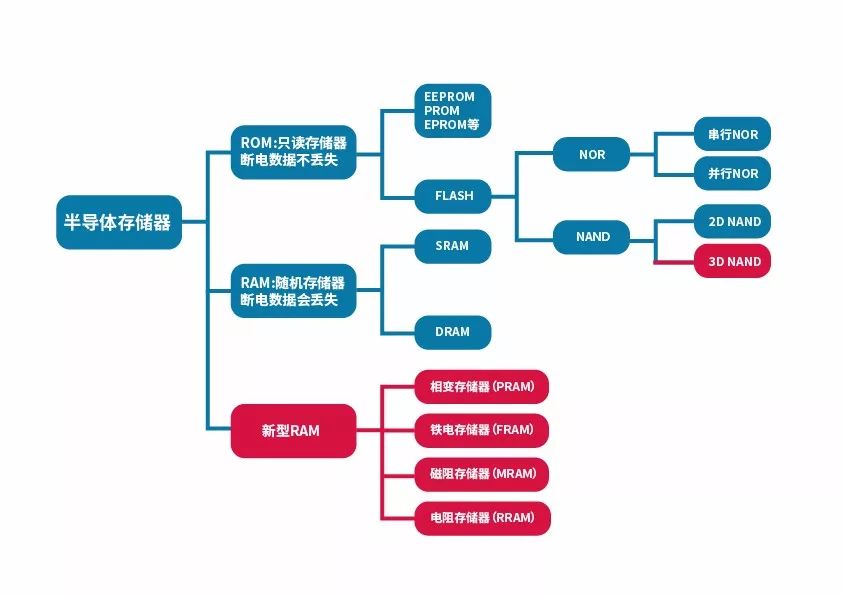
| Source: Strategic Research Office
Shanghai Institute of Microsystem and Information Technology, Chinese Academy of Sciences

Since 2016, the prices of memory have continued to rise, and to this day, supply still cannot meet demand. Memory has become one of the most关注的半导体器件之一. This article will comprehensively explore the challenges faced by both old and new memory technologies and the competition in the memory field among China, the US, Japan, and South Korea.
The second part will introduce new types of memory.
To view the first part, please click on “The Battle of Memory: Mainstream Memory”.
Although the three mainstream products currently dominate the market, they still have their own shortcomings.
DRAM: Volatile data, small capacity. Despite the excellent performance of DRAM—nanosecond-level latency, tens of GB/S bandwidth, and a lifespan close to “immortality”; however, it is a volatile memory, meaning data will be lost after a power outage, and its cost is higher than flash memory, with smaller capacity. In addition, although planar miniaturization has some distance from the physical limit, after 18/16nm, continuing to reduce size in the two-dimensional direction no longer has cost and performance advantages.
NAND: Long latency, short lifespan, planar miniaturization has reached its limit. NAND flash has advantages such as low cost (relative to DRAM), low power consumption, non-volatile, and small size, but because it requires high voltage to write data each time, which causes irreversible damage to the oxide layer, the best-performing SLC NAND has only about 100,000 read/write cycles, while the less capable MLC and TLC have read/write lifespans measured in the thousands. The situation in process miniaturization is similar to that of DRAM; after entering 16nm, the cost of 2D NAND is rising sharply, and the difficulty and cost of continuing to use planar miniaturization processes have exceeded those of 3D TSV technology. Additionally, the insulating layer must be thinned accordingly after miniaturization, and after reaching a certain thickness, electrons may experience tunneling effects under insufficient voltage, affecting chip reliability.
NOR: Small capacity, slow write/erase speed. The advantage of NOR Flash is that applications can run directly in Flash memory without needing to read the code into system RAM, hence its high transfer efficiency and fast read speed. It has high cost-effectiveness at small capacities of 1~4MB, mainly used for program storage. However, the device structure of NOR requires that all bits be written to 0 before erasing, which results in low erase speeds. Additionally, since NOR requires erasure before writing data, this also affects its write speed.
As a result, many companies and research institutions are eager to develop new types of memory that can simultaneously possess the high speed and long lifespan of DRAM and the low cost and non-volatility of FLASH.
Below are several types of new memory technologies currently receiving significant attention:
 The innovation in memory primarily has two approaches: one is the structural change from 2D to 3D, and the other is the use of new memory device structures or materials.
1. New sensors transitioning from 2D to 3D
1) 3D NAND
Currently, the mainstream process for NAND flash memory is 28nm/16nm. As the process enters the 1x nm generation, the crosstalk effect between increasingly adjacent storage cells and the electron breakdown effect caused by increasingly thin gate oxide layers have begun to affect the reliability and performance of NAND. Moreover, as we enter the 2x nm phase, the difficulty of planar miniaturization has increased significantly, and the cost advantages of miniaturization have begun to diminish, especially after 16nm, where the difficulty and cost of continuing planar miniaturization processes have exceeded those of silicon vias, thin film etching, and other 3D technologies.
In other words, whether considering performance or economic factors, continuing planar miniaturization is not a good solution. Therefore, leading NAND companies such as Samsung, SK Hynix, Toshiba, and Micron are actively developing 3D NAND technology.
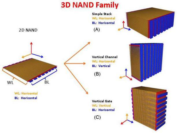
Comparison of 2D NAND (left) and 3D NAND (right)
Source: CICC, Drive Home
From 2D NAND to 3D NAND, the capacity per unit area is higher. Currently, the 32-layer 3D NAND has a capacity of 128Gb, which is on par with mainstream 2D NAND, while the 48-layer 3D NAND can achieve a capacity of 256Gb. Once the number of layers reaches 48, the power of 3D will begin to show.
Moreover, thanks to the three-dimensional stacking mode, 3D NAND can maintain a high storage density at larger storage cell sizes. Larger storage cells accept charge signals more completely, and the thickness of the gate oxide is greater, making it less susceptible to breakdown. Additionally, larger capacity NAND requires fewer retries during read/write operations, resulting in lower overall power consumption.
2) 3D DRAM
Similar to NAND Flash technology, the planar miniaturization of DRAM is also gradually approaching its limits and expanding vertically: after 18/16nm, due to the inability to continue reducing the thickness of the film and the unsuitability of using high dielectric constant (High-K) materials and electrodes, further size reduction in the two-dimensional direction no longer has cost and performance advantages. Unlike the 3D technology route of NAND, the 3D technology of DRAM is manifested at the chip level rather than the transistor level, meaning its 3D refers to 3D packaging—using TSV to stack multiple chips together. As the demand for DRAM capacity and performance in electronic products increases, the proportion of 3D DRAM is expected to rise in the future.
Similar to 3D NAND, the ability to expand in the Z direction reduces the requirements for planar miniaturization, allowing for a significant increase in the capacity of individual memory modules at larger processes. After adopting 3D packaging, connections between many chips have transitioned from horizontally intertwined copper wires to vertically oriented vias, greatly reducing interconnect line lengths, thus significantly improving post-line delay and crosstalk, which greatly aids in enhancing chip performance.
2. New memory device structures or materials
1) MRAM
MRAM stores data through magnetic polarization rather than charge. The storage unit of MRAM consists of a free magnetic layer, a tunnel gate layer, and a fixed magnetic layer. The magnetic polarization direction of the free magnetic layer can change, while the magnetic direction of the fixed layer remains unchanged. When the magnetic directions of the free layer and the fixed layer are parallel, the storage unit exhibits low resistance; conversely, it presents high resistance. By detecting the high or low resistance of the storage unit, one can determine whether the stored data is 0 or 1.
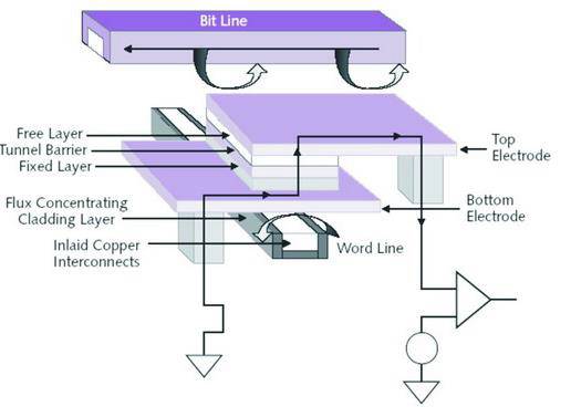 MRAM Schematic
Source: CICC, MRAM Overview (Baidu Wenku)
The research and development of MRAM is quite challenging, involving many physical principles, which is also the reason why this field has received Nobel Prizes. Magnetic tunnel junctions seem simple but are quite complex. In this structure, many materials are only a few nanometers thick, especially for MgO tunnel layers, which must be only 1.3nm and be perfect single crystals.
2) PRAM
PRAM is also a sandwich structure. The middle layer is a phase change layer (like optical disc materials, GST). One characteristic of this material is that it can transition between crystallization (low resistance state) and amorphization (high resistance state), using this change in high and low resistance states to achieve storage.
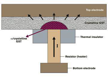
PCM Structure Diagram
Source: CICC, Science and Technology World Network
3) RRAM
RRAM appears similar to PRAM, but the principle of the transition layer is different. The phase change involves the transition between crystalline and amorphous states, while resistive switching involves forming and breaking filaments (conductive pathways) within the material to detect high and low resistance states.
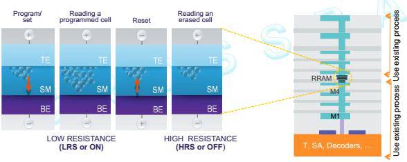
RRAM Device Unit and Storage Principle
Source: CICC, Crossbar
4) FRAM
FRAM has a structure similar to DRAM, with the basic unit consisting of a MOS transistor and a capacitor. However, the dielectric material of DRAM capacitors cannot continue to store charge after power is lost, whereas FRAM uses ferroelectric crystals that do not lose charge after power loss as the dielectric. When voltage is applied in a planar capacitor, the ferroelectric crystal forms polarized charges under the electric field. The polarized charges formed under positive voltage are lower, while those formed under negative voltage are higher. This binary stable state allows it to function as a memory.
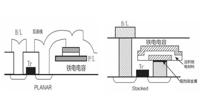
Two Mainstream FRAM Structures
Source: CICC, Microcomputer
In the field of new memory technologies, there is one noteworthy new generation memory technology called 3D XPoint, which was jointly released by Intel and Micron. This technology, developed over a decade, has achieved a combination of low cost, high speed, and non-volatility in actual products for the first time, and is described by Intel as the first qualitative breakthrough in the storage field since NAND was invented in 1989.
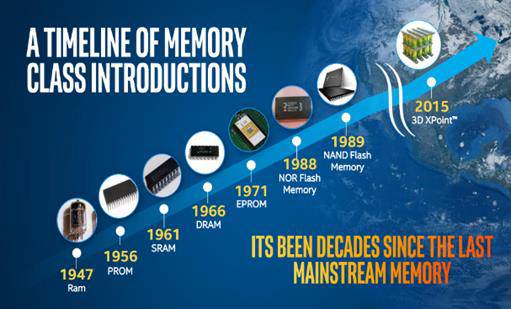
History of Memory Development
Source: CICC, Intel
The 3D XPoint technology has achieved a revolutionary breakthrough in the field of non-volatile memory. Although its speed is slightly slower than DRAM, its capacity is higher than DRAM and is 1000 times faster than flash memory. Thus, it fills a significant gap.
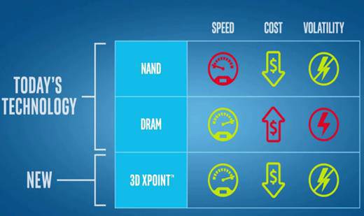
3D XPoint Combines the Advantages of NAND and DRAM
Source: CICC, Intel
The 3D XPoint uses a stacked structure, currently generally a two-layer structure.
3D XPoint Structure Diagram
Source: CICC, Intel
Compared to the previously mentioned 3D NAND, 3D NAND needs to achieve 32 layers to match the capacity of 2D NAND at 1y/1znm process (128Gb), while 3D XPoint currently only requires two layers to store 128Gb of data at a 20nm process. Thus, its potential for expansion in the Z direction is significantly greater than that of 3D NAND.
Intel and Micron have been suppressed by companies like Samsung, SK Hynix, and Toshiba in the memory field for many years. The joint launch of this disruptive new type of memory undoubtedly captures a lot of attention that was previously focused on 3D NAND, which is heavily promoted by Samsung and SK Hynix.
Conclusion
In recent years, driven by market demand and emerging technologies, the transition from traditional memory to new types of memory has accelerated. Overall, the most promising developments currently are 3D NAND, 3D DRAM, PRAM, and 3D XPoint, while others remain mostly at the laboratory sample stage. The reasons for this phenomenon are mainly twofold: first, the development difficulty of RRAM, FRAM, MRAM, and other memories is high; second, 3D NAND and 3D DRAM involve relatively few new technologies and materials, making development relatively simple. Some companies have already achieved mass production, and these products have shown significant performance improvements compared to the previous generation of 2D flash memory.
It is expected that in the coming years, the main battlefield for major memory manufacturers will be in 3D NAND, and the next generation of memory after 3D NAND is likely to be 3D XPoint.
In the next part, we will bring you “The Battle of Memory (III): The Market Landscape of Memory in China, the US, Japan, and South Korea”, stay tuned.
This article is original from the SIMIT Strategic Research Office. For reprints, please contact [email protected]